

Dr. Dimiter Prodanov from Imec gives an end-user industrial perspective on the vital role of nanomaterials in today’s semiconductor industry and their safe use
Nanomaterials are broadly defined as those materials that have a certain percentage of particles at the nanoscale, between 1 and 100 nanometres1. While the size cut-off used in the definitions is somewhat arbitrary, it nevertheless conveys the important fact that properties of materials with nanoscale features (e.g. nanoforms) can substantially differ from the properties of “macro” materials in bulk.
Nanoforms can have desirable characteristics, such as the increased strength of the material, modified chemical reactivity or electrical properties. These features offer possibilities for new applications in a broad range of sectors; for example, in medicine (e.g. detection of genetic sequences using DNA-tagged gold nanoparticles); environment (e.g. waste-water treatment with carbon nanotube filters); or energy production (e.g. solar cells using silicon nanocrystals).
At the same time, the use of manufactured nanomaterials in various commercial applications raises questions about potential unintended risks to both humans and the environment: for it is known that particles of nanometre size can get deposited in the lungs, pass easily through alveoli or even get dispersed in the body.
Top-down and bottom-up approaches to nanotechnology
Nanotechnology intentionally uses desirable properties of materials at the nanoscale to deliver economically beneficial effects. From a technological perspective, there are two complementary approaches: top-down and bottom-up processing. While the bottom-up approach can be broadly identified as particle synthesis or self-assembly, the top-down approach can be thought of as growth or deposition on surfaces. An example of the latter can be found in the micro- or nanoelectronics industry. Nanomaterial manufacturers typically employ bottom-up approaches, while end-user industries incorporate engineered nanomaterials into macroscopic objects, for example in products like computer chips, tires and sportswear.
From an industrial end-user perspective, modern nanoelectronics employs technologies offering unprecedented control of the properties of the finished product in large volumes. Semiconductor processing today uses a variety of materials, as companies seek to further improve devices’ performance to meet an increasing market demand.
This innovation, in turn, leads to some new materials and nanoforms being introduced in process technology. Typically, the product development runs ahead of the establishment of metrics for the occupational and environmental hazards related to these materials. Since nanoelectronics inherently deals with novel materials and processes, the challenge is the lack of information leading to uncertainty in risk grouping and governance.
Other industries are facing similar concerns due to the development of new materials; for example, the pharmaceutical and the cosmetics industries, although on longer time frames. While there is no golden standard for risk assessment and management, several pragmatic systems have come into being. All these approaches implement the precautionary principle as a way of avoiding underestimation of the risk.
International efforts and EU regulations
Understanding the properties of engineered nano-materials and how they behave in living systems, such as the human body, is a relatively new area of scientific study. It becomes increasingly clear that harmful properties of nanoforms sometimes do not correlate with the toxicological profile of the bulk materials. One of the challenges in that respect is the identification of the best metric for toxicological assessment. A related challenge is how to define a ‘nanomaterial’.
To address these challenges international bodies, such as the European Union, have orchestrated substantial efforts. As part of this ongoing effort, the European Commission funds the NanoStreeM project. The NanoStreeM project is funded under H2020 grant agreement 688194 of the European Commission. The goals of the project are to promote good practices by identifying applicable standards – and to identify gaps in methodologies and directions for further investigations to support governance of the occupational risk induced using nanomaterials in the semiconductor industry.
Vision
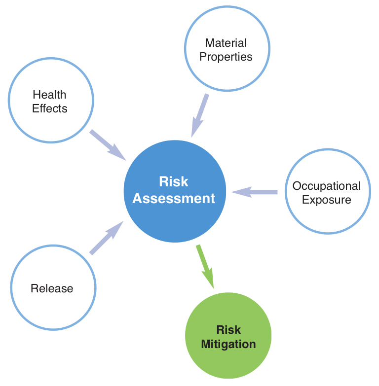
A holistic view of the nano-hazard and the related process risk is crucial for successful integration of nanosafety aspects into the overall risk management methodology. Material properties, health effects, the potential of release and occupational exposure are principal aspects for successful risk mitigation (see Figure 1). The NanoStreeM consortium combines unique expertise throughout the research and development chain: from the academic labs via technology development through the semiconductor application side.
The consortium partners set forth the following objectives:
- Build inventories of materials, research topics and directions relevant for nanomaterial use and exposure in nanoelectronics manufacturing.
Activities grouped along this direction will allow the semiconductor industry to get further insight in emerging risks and continue taking a pro-active approach in the control of risks of using engineered nanoparticles and in the potential release of incidentally generated nanomaterials. This direction also identifies the specific novel engineered nanomaterials, which may be introduced in the future; for example, rare earth elements, transitional metal nanowires, carbon nanotubes or graphene.
- Identify gaps in knowledge and methodologies to assess the risk of engineered nanomaterials used in semiconductor manufacturing or incidentally released as by-products of the manufacturing process.
Activities along this direction aim to identify suitable risk assessment tools developed in the context of other industries or funded projects. The identification of commonly missing information about physical, chemical or toxicological properties of the materials in scope may be the input for further studies in the growing field of nanosafety. Another important outcome will be the comparison of current practices of medical supervision with respect to occupational exposure to engineered nanomaterials.
- Apply results for better governance of the emerging risks.
We identify safety training as a crucial aspect of prevention of accidents and exposure. To this end, the consortium develops a generic Nanosafety training package applicable to the semiconductor industry. This is an outcome, which can allow a lasting impact beyond the duration of the project. More information is available on the project website at www.nanostreem.eu.
1 EC definition: at least 50% primary particle threshold, except in specific cases.
Please note: this is a commercial profile
Dr. Dimiter Prodanov MD, PhD
EHS Life Science Partner
Imec
Tel: +32 162 818 40
More About Stakeholder
-
 imec – imec.iStart
NanoStreem strives for better understanding of the occupational hazards related to the use of nanomaterials, and the better governance of the risks related to of the manipulation of nano-materials
Editor's Recommended Articles
-
 Must Read >> Nanomaterials for energy storage: Powering our world
 -

-