H. Alan Mantooth, Distinguished Professor at the University of Arkansas, guides us through power electronic modules, which form the basis of grid modernization
For the past 25 years, the University of Arkansas Power Group (UAPG) and its collaborators have advanced the field in power electronics packaging research, development, and commercialization.
Formed in 1991 under DARPA funding, the High-Density Electronics Center (HiDEC) at the University of Arkansas has been at the forefront of electronics packaging for almost 35 years. For the majority of that time, there has been an intense effort on packaging power semiconductor devices into what is commonly known as power modules.
These electronic assemblies are designed to create a compact, high-current power switching configuration by connecting several devices in parallel to meet the demands of electric power grids and heavy industry applications. Of course, these began with silicon power devices, which continue to this day.
R&D: Power electronic modules for grid modernization
However, over the past two decades, the emergence of silicon carbide power devices has led to a tremendous level of R&D and commercialization efforts because of the higher switching efficiency of this material system as compared to silicon. This higher switching efficiency results in higher efficiency power converters requiring less thermal management than silicon. These attributes are ideally suited to address the booming demand for electrical power processing needed by data centres.
HiDEC is a part of the UA Power Group. This R&D activity has led to the development of new power module solutions at the UA, as well as a number of its collaborators. One of these, a spinout company from the UAPG, was Arkansas Power Electronics International, which was acquired by Cree (now Wolfspeed) in 2015.
Other collaborators have included industry stalwarts such as Rohm Semiconductor, onsemi, Toyota, Ford, American Electric Power, Southwest Power Pool, Midwest Independent Systems Operator, General Electric, Leonardo DRS, G&W Electric, Eaton, Con Edison of New York, and many others through the NSF Center on GRid-connected Advanced Power Electronic Systems (GRAPES).
This activity has been performed at times in partnership with the University of Wisconsin – Milwaukee and the University of South Carolina as part of GRAPES; the University of Illinois, Urbana-Champaign (UIUC), Stanford University, and Howard University as part of the NSF Engineering Research Center on Power Optimization of Electro-Thermal Systems (POETS); and UIUC, UWM, Oak Ridge National Laboratories, and Arizona State University under ARPA-E funded projects.
New power module architectures advancements
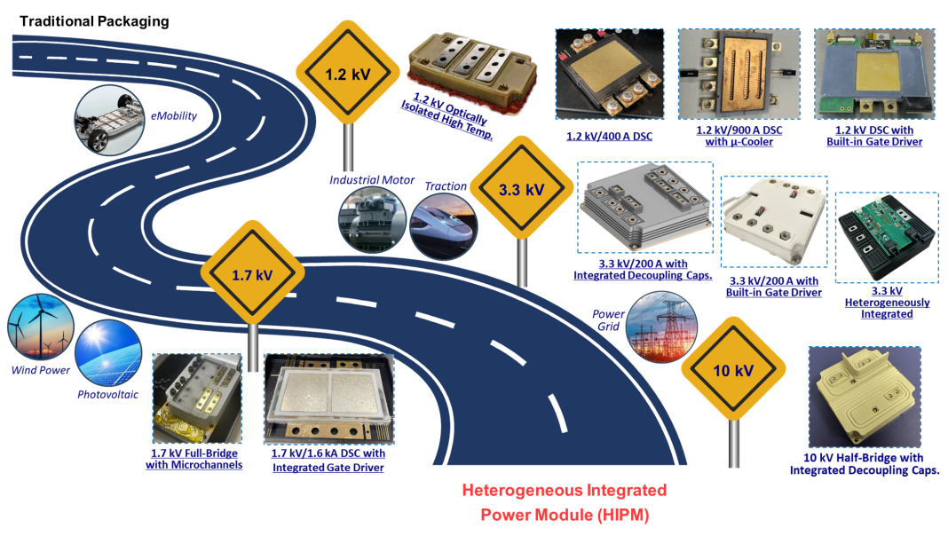
These efforts have led to new power module architectures with voltage ratings from 650 V through 10 kV and current ratings up to 1.6 kA. The UAPG roadmap on power module development is illustrated in the figure opposite. This figure illustrates several modules developed over the last ten years, some of which have been transferred to industrial partners for further development into commercial offerings. It begins from the traditional packaging concepts and illustrates how the group has evaluated various forms of heterogeneous integration concepts into modules to enhance performance.
Among these shown at the 1.2 kV level are integrated optical isolation, integrated gate driving, integrated thermal management, and 3D wire bondless modules. Progressing upwards to 1.7 and 3.3 kV includes both gate driving and embedded passive elements to ensure low inductance and current sharing in modules containing more massively paralleled devices. Finally, at the 6.5 and 10 kV levels, substantial effort has been made to reduce common mode capacitances that lead to EMI concerns.
Because of the material characteristics of silicon carbide, the resulting power semiconductor devices made from SiC can switch faster because of lower device capacitances. This faster switching means that inductive parasitics within the module need to be controlled more closely than in silicon power modules to ensure signal integrity.
Otherwise, the voltage and current waveforms will appear noisier, which leads to device stress, lack of reliability, and needless generation of electromagnetic interference (EMI) that can impact surrounding circuitry, including those that drive and control these very power semiconductor devices.
To avoid this phenomenon, UA researchers have also developed state-of-the-art design tools that allow them to optimize the layout by minimizing electrical parasitics. This optimization also helps to manage the thermal coupling of devices that might be too close to one another, thus striking a Pareto compromise between thermal and electrical characteristics.
Further research has involved including reliability constraints and models into the framework that provide an electro-thermal-mechanical co-optimization for the module.
Transforming power electronics converters at the electric power grid scale
The latest activity being pursued begins to integrate all of these types of features into a single 3.3 kV module platform that can switch at speeds in excess of 250 V/ns and 100 A/ns, leading to very low loss modules and converters, while minimizing reliability concerns surrounding partial discharge and EMI generation. This architecture has the potential to scale to higher voltage nodes and make a transformative difference in power electronics converters at the electric power grid scale.


