
Elisabetta Fiordaliso of DTU CEN discusses Nanowire technology and how it works, something which is decreasing the dimensions of our electronic devices more and more.
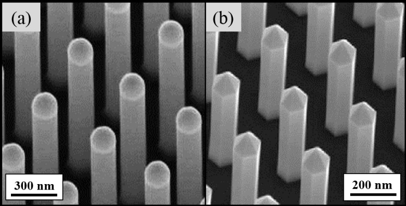
The density of integrated electronic components in the semiconductor industry continues to increase, resulting in shrinking dimensions of individual devices. Many different semiconductor materials are synthesized in nanowire (NW) form. NWs are structures with length from few hundred nanometers to microns and thickness significantly smaller compared to its length. The cross section of a NW can be round, hexagonal or polyhedron, according to the crystallography of the used material. Figure 1 shows scanning electron micrographs (SEM) for Si and GaN NWs, having different geometries.
Semiconductor NWs are employed as building blocks for high performance nanoscaled devices because they impart various benefits to electronic and photovoltaic devices compared to their thin film counterparts. For instance, they can be grown with no crystal defects and they can accommodate large lattice mismatch strain, enabling new heterostructure material combinations with atomically sharp interfaces [1].
Challenges of nanowire sizes
One of the major challenges towards nanometre-size scaling of electronic devices based on semiconductor NWs is achieving controlled doping of NWs at the atomic level. Doping is the intentional addition of atomic impurities in a material to produce positive (p-type) or negative (n-type) semiconductors. This is done to accurately manipulate the electrical, optical, and magnetic properties. For silicon, elements such as P, As and Sb are donors as they have one more valence electron than silicon and make the silicon n-type. Likewise, elements such as B, Al and Ga are acceptors and make the silicon p-type. Typical methods of doping semiconductors are ion implantation, in-situ doping where the dopants are introduced into the NWs during growth, and chemical approaches such as chemical vapor deposition (CVD) and spin-on doping (SOD).
The doping in NW can be measured with different methods, including photoluminescence and conductivity, four-point probe resistivity, Raman spectroscopy, secondary ion mass spectrometry and atom probe tomography. At DTU Cen we can use off-axis electron holography to measure the doping in nanowires. Off-axis electron holography is a transmission electron microscopy (TEM) technique that measures a spatially-resolved phase contrast from a specimen due to an electrostatic potential. This technique enables to detect active dopants and provide direct visualization of doping distribution and p-n junctions at the atomic scale [2-4]
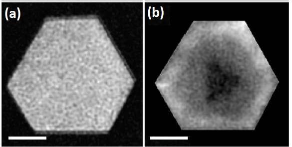
An example of a holographic measurement across an in-situ doped core-shell GaAs NW is shown in Figure 2. Cross-sectional specimens for off-axis electron holography are prepared perpendicular to the growth direction of the NWs using focused ion beam (FIB) milling, which is a technique also available at DTU Cen. The amplitude image (Figure 2 (a)) is equivalent to a conventional TEM image, whereas the phase image (Figure 2 (b)) is sensitive to the presence of electrostatic potentials inside the NW caused by active dopants. The active dopants show a remarkable azimuthal distribution, which is attributed to preferred incorporation along 3-fold symmetric truncated facets of the NWs during growth [2]. These results reveal an unexpected doping mechanism that has not been predicted nor observed previously.
References
[1] Kavanagh, K. L., Semicond. Sci. Technol. 25.2 (2010): 024006.
[2] Tavakoli D., et al., Nano Letters 17.10 (2017): 5875.
[3] Cooper, D., J. Phys. D: Applied Physics 49.47 (2016): 474001.
[4] Yazdi, S., et al. Ultramicroscopy 152 (2015): 10-20.
Postdoc Elisabetta Maria Fiordaliso
Center for Electron Nanoscopy
DTU Cen, Technical University of Denmark
Tel: +45 4525 6494
e.fiordaliso@cen.dtu.dk


