")
Prof. Singisetti at the University at Buffalo explains why gallium oxide semiconductor could be a key player in the AI transformation of society
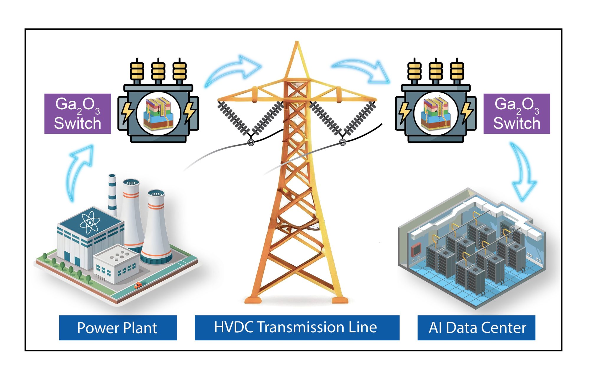
The release of ChatGPT in 2022 has led to an explosive increase in Artificial Intelligence (AI) applications and investments. The large language model (LLM) AI has proven to be extremely capable of performing complex tasks across a broad range of topics, yielding enormous economic benefits. This has led to massive investments in AI data centers. However, a significant challenge is the substantial energy demand of AI to perform even basic tasks. The anticipated demand for AI energy has bolstered nuclear power as a reliable energy source. The increased demand has also led to plans for high-voltage transmission lines in the US. As the AI data centers proliferate, power semiconductors will play a crucial role in integrating the new energy sources into the grid.
The use of high voltage for efficient energy transmission was realized at the dawn of electricity production and transmission. While AC transmission provided an easy way to achieve high voltages, high-voltage DV (HVDC) transmission was developed with the introduction of power semiconductor devices. HVDC transmission lines can transport gigawatts (GW) of power at megavoltages (MV). While series-connected thyristors are currently used, high-voltage 10-20kV power MOSFETs can significantly reduce complexity and cost. Specifically, gallium oxide is well-positioned to meet these requirements due to several fundamental material and technological advantages, as described below.
Gallium oxide is a promising ultra-wide bandgap (UWBG) power semiconductor
Gallium oxide is one of several ultra-wide bandgap (UWBG) semiconductors that are currently under investigation for power applications. The monoclinic β phase of gallium oxide has an energy bandgap of ~ 4.8eV, nearly five times the bandgap of silicon. The large bandgap enables higher voltage operations required for grid-level power transmission. Besides the bandgap, several other key factors make gallium oxide advantageous for transitioning from academic laboratories to field applications. The similarity between silicon and gallium oxide is one key advantage. The lessons learned from the adaptation of gallium nitride and silicon carbide can be applied to this emerging technology, facilitating an easier transition from lab to fab.
While several materials have large band gaps, what differentiates insulators from semiconductors is the availability of shallow dopants, which make them conduct at room temperature. Gallium oxide has multiple shallow dopants (Si, Ge, Sn), making it a promising UWBG power semiconductor. The intentional doping density in gallium oxide can be controlled over multiple orders of magnitude, ranging from 1015 cm-3 to 1020 cm-3. For high-voltage applications, it is highly critical to achieve intentional doping in the 1015 cm-3 range. This level of purity is significantly lower than that in artificial gems, which highlights the challenges for any UWBG semiconductor. Additionally, the extremely pure materials need to be synthesized at low costs. High-quality gallium oxide films can be grown cost-effectively due to the availability of melt-growth methods for substrate production and the resultant homo-epitaxy.
The role of low-cost substrates for vertical power devices cannot be overstated. As any emerging power technology must compete with silicon power electronics, the cost becomes a deciding factor, as the cost of silicon power electronics is extremely low due to decades of technological development. The substrates play a dual role, providing both a mechanical anchor and a low-resistance back contact for power devices. Gallium oxide can be grown using a variety of melt growth methods, which are extremely cost-effective due to high material utilization. Within a short time span, four-inch gallium oxide substrates are available, while six-inch substrates are demonstrated. The substrate size can be eight inches if there is sufficient commercial demand. Moreover, the substrates can be highly doped with Sn, Si, or Ge to reduce the substrate resistance. Substrate resistance contributes significantly to total resistance in commercial silicon carbide devices; thus, it is imperative to develop high doping in UWBG substrates.
Another parameter in the power device manufacturing chain is the availability of gate oxides and reliable methods for etching, implanting, and forming contacts. Both silicon dioxide and aluminium oxide have been used in multi-kV gallium oxide transistors. Gallium oxide can be etched in standard chlorine-based reactive ion etch systems. Ion implantation has been successfully used for forming source- drain regions. The annealing temperatures are below 1000 °C, which reduces the cost of the furnaces. These advantages make it easy to integrate gallium oxide fabrication into existing silicon fabs. In fact, gallium oxide fabrication can increase the utilization rate of existing WBG foundries, providing further avenues for cost reduction. Besides these, there have been well-calibrated transport models that can be used in commercial device simulators.
Gallium oxide diodes and MOSFETs have demonstrated operation at 10 kVs
Due to the advantages mentioned above, gallium oxide diodes and MOSFETs with 10kV operation have been demonstrated. Furthermore, there have been reports of short-circuit robustness, UIS testing, and switching robustness. Small area MOSFETs and diodes with power device figure of merit of 1 GW/cm2 have been demonstrated. All these indicate the electrical performance potential of gallium oxide high-voltage devices.
Finally, a well-known challenge for gallium oxide is its low thermal conductivity, which arises from the crystal structure. This challenge could be addressed for grid-level applications, as high-voltage installations currently use advanced cooling techniques for thyristors. The same cooling infrastructure could be used for gallium oxide power devices. Moreover, advanced packaging techniques, such as double-sided cooling, have been demonstrated to be effective for experimental gallium oxide devices.
In summary, gallium oxide possesses both fundamental material properties and key technological advantages, particularly in 10-20kV power MOSFETs. The availability of substrate can provide key value propositions over incumbent power device technologies. At the same time, the rise in AI power demand can provide a needed market incentive. While these predictions are based on sound rationale, the final proof is in the pudding. Gallium oxide transistors must stand on their own and show the thermal robustness required for grid applications.