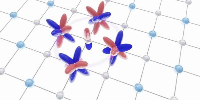
Columbia University researchers have discovered a new way to create quantum materials. By utilising the chemistry of atomic orbitals, they’ve found a novel source of “frustration” that leads to complex quantum behaviours
Scientists at Columbia University have announced a groundbreaking discovery that demonstrates how the inherent chemistry of a material, specifically its atomic orbitals, can be a new source of “frustration” leading to complex quantum phenomena. This new perspective, detailed in a recent publication in Nature Physics, moves beyond traditional reliance on crystal lattice geometry, opening up potential for designing materials with desired quantum properties.
Experts in physics and chemistry were brought together to explore the new material Pd5AlI2. “It’s a classic Columbia story—multiple groups in physics and chemistry came together to work on this new material, and we found exciting new results about how electrons move,” explained Aravind Devarakonda, an applied physicist at Columbia Engineering and lead author of the study.
Beyond geometric frustration
For decades, the concept of “frustration” in quantum materials has been primarily linked to geometry. In classical physics, electrons repel each other, but in certain quantum scenarios, they can be forced to pair up, leading to intriguing behaviours like superconductivity or unique forms of magnetism. This pairing often occurs when electrons in a material cannot find a stable, low-energy configuration due to the physical arrangement of atoms in the crystal lattice, particularly in structures like triangles or squares. These geometrically frustrated materials, however, are rare.
Pd5AlI2, a metallic and air-stable material that can be peeled into atom-thin layers, is changing this narrative. Its initial examination revealed a seemingly straightforward lattice. However, preliminary measurements by Devarakonda uncovered an electronic feature characteristic of a geometrically frustrated structure known as a Lieb lattice, which is made of squares and had largely been confined to theoretical models.
The “Eureka moment” arrived when theoretical physicist Raquel Queiroz connected Devarakonda’s observations to the material’s chemistry. It was discovered that the material’s atomic orbitals – the regions where electrons are most likely to be found around an atom – combine to form a checkerboard pattern that precisely mimics the geometry of a Lieb lattice. “We’ve found an entirely new way to think about frustration, one that combines how chemists think about chemical bonds with how physicists think about crystal lattices,” stated Columbia chemist Xavier Roy, whose lab synthesised the new metal. This revelation means that the material’s internal chemistry, not just its external atomic arrangement, is the driving force behind its frustrated electron motion.
Flat bands: The key to quantum wonders
The curious electronic feature observed by Devarakonda turned out to be a coveted electronic flat band. Flat bands are electronic structures where electrons are all forced to share the same energy, creating an inherently unstable yet highly intriguing state. This unique configuration is a fertile ground for unusual quantum behaviours, including the potential for high-temperature superconductivity – a holy grail in materials science that could revolutionise energy transmission and storage.
The ability to induce frustration through orbital configurations offers a powerful new tool for scientists. This approach provides a simpler and potentially more widespread pathway to creating materials that exhibit flat bands, moving beyond the limitations of rare geometrically frustrated structures.
Applications and beyond for quantum behaviours
The Columbia team is already pushing the boundaries of this discovery. Devarakonda is actively manipulating samples, for instance, by physically stretching them, to explore ways to control and enhance these quantum behaviours. As a layered crystal, Pd5AlI2 has been successfully peeled down to a single atomic layer, opening up exciting possibilities for combining it with other 2D materials to engineer entirely new forms of physics. Its metallic nature and stability in thin layers are particularly advantageous, allowing for the creation of even more compact stacked structures.
The potential applications of this research are significant. It could lead to the development of novel quantum sensors capable of recording subtle changes in their environment by exploiting the trapped electrons’ properties, such as their spin direction. Furthermore, insights gained from Pd5AlI2 could contribute to the creation of rare-earth-free, room-temperature magnets, addressing the growing concerns about the cost and availability of rare-earth elements crucial for modern technologies like electric motors and wind turbines.
While Pd5AlI2 itself is not inexpensive, the researchers are optimistic about leveraging AI techniques to rapidly identify other crystals that might possess this “orbital frustration” within their chemical bonds. “The possibility of frustrated hopping from orbitals was articulated theoretically, but now we have a concrete example,” said Devarakonda. “There are so many models that people have come up with over the decades, but now we can use our newfound insights about lattices and orbitals to chase them from a different angle.”


