A new approach to producing graphene could revolutionise its use in electronics, sectors and energy storage
Graphene has always fascinated scientists and engineers due to its massive strength, conductivity and flexibility.
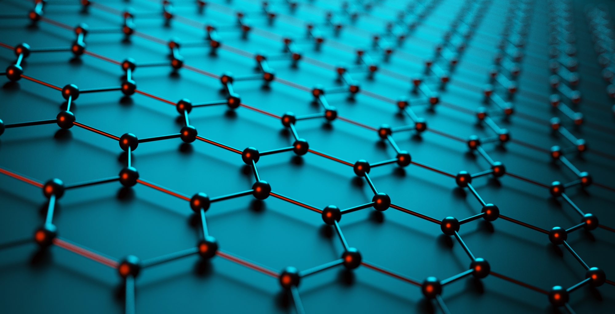
Traditionally, the goal has been to produce perfect graphene sheets with flawless hexagonal arrangements of carbon atoms. However, new research suggests that introducing intentional “defects” could actually make graphene more useful.
A team of scientists from the University of Nottingham, the University of Warwick, and Diamond Light Source has developed a new, single-step method for growing graphene that includes specific structural imperfections. These controlled defects improved the materials’ properties, making it more adaptable for a range of real-world applications.
Turning flaws into functional features
In most materials science, defects are something to avoid. They often weaken materials or interfere with their intended properties. However, in this case, researchers took a different approach: they intentionally introduced defects. These imperfections altered the chemical and electronic behaviour of graphene, enhancing its ability to adhere to other materials, act as a catalyst, and direct gases. All of which are valuable traits for industries working with sensors, batteries or semiconductors.
By carefully selecting the starting materials and controlling the growth conditions, the team was able to embed a specific type of defect in the graphene. These defects involve the replacement of the regular six-carbon atom rings with a mix of five- and seven-membered rings. The result is a material that behaves differently from perfect graphene.
The role of Azupyrene
One of the main parts of this new process is a molecule called Azupyrene. Its natural shape closely mimics the kind of irregular ring structure researchers aimed to introduce into the graphene.
When used during the growth process, Azupyrene helps form graphene-like films that are rich in these controlled defects. One of the advantages of this method is the ability to fine-tune the number of defects by simply adjusting the temperature during growth. This level of control is crucial for tailoring the material’s properties for specific uses.
One of the advantages of this method is the ability to fine-tune the number of defects by simply adjusting the temperature during growth. This level of control is crucial for tailoring the material’s properties for specific uses.
Scalable and transferable
A significant step forward was demonstrating that this new form of defective graphene could be transferred onto various surfaces while retaining its unique structure. This means it could be integrated into existing technologies and manufacturing processes, making it highly attractive for practical applications.
This achievement was made possible through collaboration with researchers at the Graphene Institute in Manchester, involving advanced characterisation techniques to confirm the presence and impact of the defects.
International collaboration and advanced tools
To fully understand how the defects altered the graphene’s behaviour, the team used tools that included atomic-scale imaging, spectroscopy, and high-powered computational modelling. These experiments took place at research facilities across Europe, including the Diamond Light Source in Oxfordshire, the MAX IV laboratory in Sweden, and the ARCHER2 supercomputer in the UK.
This international effort combined experimental and theoretical expertise, enabling researchers to investigate the atomic-level mechanisms underlying defect formation and their impact on the material’s performance.
A new direction for graphene research
The discovery reveals a shift in how scientists perceive graphene. Rather than searching for perfection, this method embraces an engineer’s imperfections to improve the material’s function. The ability to customise graphene’s properties opens new possibilities for its use in electronics and sensing technologies,


