
Exploring the fundamentals of electron matter interactions to turn radiation damage into an exciting opportunity for nanotechnology
Imaging nanoscale phenomena in transmission electron microscopy requires the irradiation of our target sample with high-energy (60-300 keV) electrons. The interaction between these electrons and the atoms within the sample provide the signals we use to gain physical knowledge. However, they also inflict damage on the specimen, limiting acquisition and complicating the interpretation of structural and chemical data. Microscopists targeting inorganic/hard materials can generally ignore these complications. In other cases, for example when studying catalytic reactions or soft matter, a great deal of caution is required.
At the National Centre for Nano Fabrication and Characterization at Technical University of Denmark (DTU Nanolab), we pay special attention to electron matter interactions, and focus our efforts towards their deep scientific understanding in view of turning them into a useful tool for a variety of applications in nanotechnology. No other project demonstrates it better than Organic Ice Lithography, where we exploit electron matter interactions to trigger the nanoscale transformation of a frozen layer of volatile organic molecules into a solid product.
Organic Ice Resist Lithography (OIRL) is a new approach to electron beam based nanofabrication, developed at DTU Nanolab [1][2]. The goal of electron beam lithography (EBL) (Figure 1(a)) is to create a desired pattern in a sacrificial material called resist. The portion of the resist that is irradiated by an electron beam undergoes chemical changes, driven by two competing processes: chain scission and crosslinking (Figure 1(b)). Chain scission is the fragmentation of molecules into smaller units, while crosslinking involves molecular units joining together. After exposure, the resist is immersed in a suitable chemical called developer. Chain scission reduces resist solubility; crosslinking does the opposite. Depending on which process dominated during the exposure, either the exposed or the unexposed areas will be dissolved by the developer (Figure 1(a)).
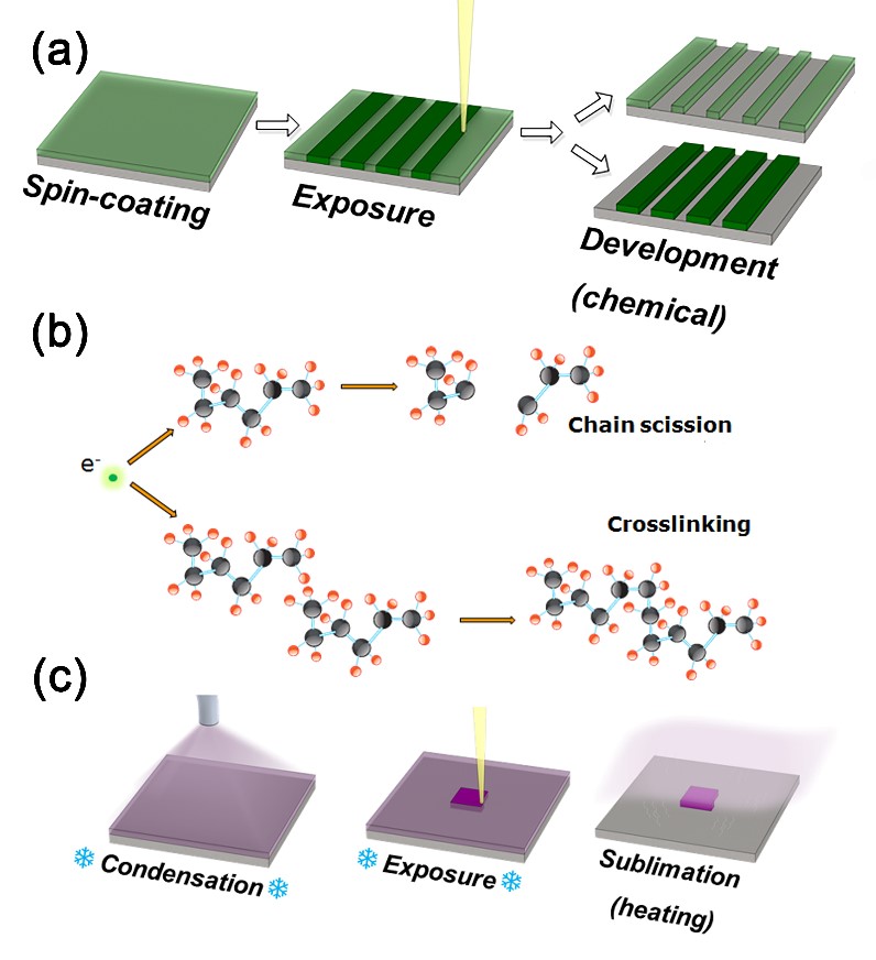
In OIRL, the organic ice resist material is condensed from vapor directly on a substrate held at cryogenic temperature (Figure 1(c)). With all the molecules we have tried so far (1-pentanol, n-nonane, anisole), the exposure process is dominated by crosslinking of the molecules. However, it is not the change of solubility that matters here, but the increase in the critical sublimation temperature of the exposed areas. Therefore, the unexposed areas are removed simply by heating the substrate to room temperature. This approach offers several advantages over existing EBL methods. First, all process steps take place in a single instrument; repeating multiple cycles of condensation-exposure-heating steps enables the effective and precise fabrication of 3D layered structures. Second, it is easy to deposit the resist uniformly on any surface – porous, grooved or curved. Finally, no chemicals are involved other than the resist precursor; this reduces residual contamination and chemical pollution of a sample.
Our first publication in 2017 [1] showed OIRL in action and demonstrated that simple organic molecules such as 1-pentanol, nonane and anisole can be used as resist materials. The next step was to establish and explore the link between resolution performance of OIRL and the chosen precursor, in particular its initial molecular weight, and the beam exposure parameters.
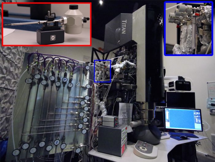
Figure 2: (a) FEI TITAN E-Cell 80-300 ST Environmental TEM, equipped with gas cell and gas mixing system. (Right inset) Glass vial with organic precursor attached to one of the gas lines. (Left inset) Cryo Gatan TEM sample holder.
This is where transmission electron microscopy came in. The optics offered by TEM allows to minimize the instrumental limitations imposed on patterned feature size. This strategy was implemented by scientists from Brookhaven National Laboratory who used an aberration-corrected TEM in scanning mode to pattern sub-4 nm features on EBL resists [3]. In that case, the TEM was only used for e-beam exposure step. Our task was more complicated, since all process steps had to be carried out in a single instrument. Luckily, at DTU Cen we have an Environmental TEM (ETEM) (Figure 2). The sample in the ETEM is isolated from the column by two pressure-limiting apertures[4]. The apertures together with differential pumping lines attached between them allow to image the sample under elevated pressures. ETEM is also equipped with gas mixing manifold system, which delivers a stable pressure stream of a desired gas into the microscope column. To turn the ETEM into an ice lithography instrument we filled the glass vial with organic precursor and attached it to one of the gas lines (Figure 2, right inset). The vapor condensed on a substrate mounted on a cryo-transfer Gatan sample holder cooled down to liquid nitrogen temperature (Figure 2, left inset).
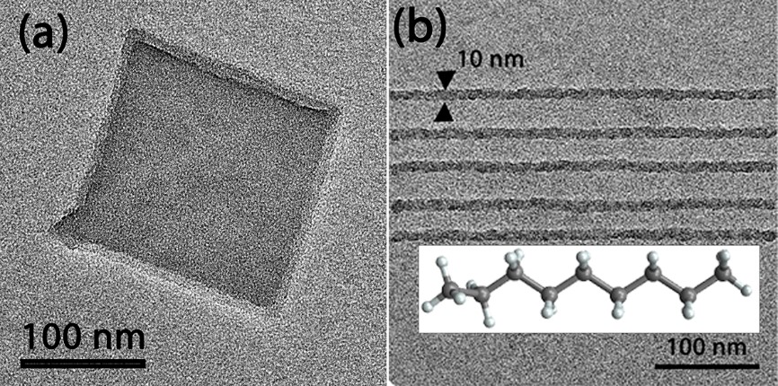
After a long process of optimizing ice deposition and exposure parameters, we successfully patterned features on n-nonane organic ice (Figure 3 (a)), including 10-nm parallel lines (Figure 3 (b)). Currently we are focusing our effort on exploring other OIR materials and, most importantly, on understanding why and how OIRL works. In our most recent publication [5] we present our results on patterning linear hydrocarbon OIRs and discuss how the initial molecular weight of the precursor affects the exposure process and defines the feature size of the resulting structures.
We believe that OIRL has a bright future and can bring many benefits to applications that require fabrication of 3D structures, patterning of complex surfaces and biocompatibility. We are also certain that it will shed light on many yet unanswered questions concerning interaction of organic matter with the electron beam.
[1] W. Tiddi, A. Elsukova, H. T. Le, P. Liu, M. Beleggia, and A. Han, “Organic Ice Resists,” Nano Lett., vol. 17, no. 12, pp. 7886–7891, Dec. 2017.
[2] W. Tiddi, A. Elsukova, M. Beleggia, and A. Han, “Organic ice resists for 3D electron-beam processing: Instrumentation and operation,” Microelectron. Eng., vol. 192, pp. 38–43, May 2018.
[3] V. R. Manfrinato, L. Zhang, D. Su, H. Duan, R. G. Hobbs, E. A. Stach, and K. K. Berggren, “Resolution Limits of Electron-Beam Lithography toward the Atomic Scale,” Nano Lett., vol. 13, no. 4, pp. 1555–1558, Apr. 2013.
[4] P. Mølgaard Mortensen, T. Willum Hansen, J. Birkedal Wagner, and A. Degn Jensen, “Modeling of temperature profiles in an environmental transmission electron microscope using computational fluid dynamics,” Ultramicroscopy, vol. 152, pp. 1–9, May 2015.
[5] A. Elsukova, D. Zhao, A. Han, M. Beleggia “Effect of molecular weight on the feature size in organic ice resists”, Nano Lett., 18 (12), pp 7576–7582, Nov 2018

Anna Elsukova
Postdoctoral researcher DTU Nanolab, Technical University of Denmark


