
Shima Kadkhodazadeh of DTU Nanolab provides insight into Photonic Nanostructures following research conducted at the Technical University of Denmark
Humanity has always been fascinated by light and its interaction with matter, manifested by the ageless desirability of precious stones. Today, nanostructures exploiting optical phenomena are prevalent in fields ranging from telecommunications to solar cells, catalysis, biological sensing and medical diagnostics. A key requirement for future progress in these technologies is obtaining better understanding of the structure – functionality relationship of their constituent components on the nanometre scale. This calls for characterisation methods that are capable of probing structure and properties with nanometre spatial resolution and beyond. A powerful tool for nanoscale characterisation is transmission electron microscopy (TEM). Today’s aberration-corrected TEMs can routinely image structures with atomic resolution. In aberration-corrected scanning TEM (STEM) electrons can be focussed into a probe below 1 Å in diameter, allowing both imaging and chemical analysis to be carried out with atomic resolution. Other characteristics such as strain, polarity and electric field strengths can also be measured in today’s TEMs, all of which influence the optical performance of structures.
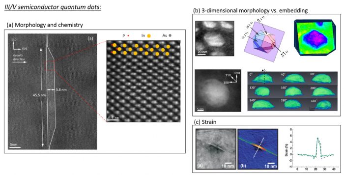
Our studies of photonic nanostructures have included III/V semiconductor quantum dots. Low dimensional semiconductor structures are of interest in a number of fields, due to their characteristics that differ from those of the bulk, and which can be manipulated by controlling their structure and chemistry. Quantum dots have dimensions so small that quantum mechanical effects result in the quantisation of their electronic density of states in 3 dimensions. The exact configuration of the electronic states and subsequently, the optical properties of the quantum dots are largely determined by their structure and chemistry. Thus, a significant step in optimising their performance and synthesis is understanding their subtleties on the nanometre or even atomic scale. Our studies have included atomic resolution imaging to determine the morphology and chemical distribution1, 3-dimensional reconstruction of morphology2 and strain measurement3 (Figure 1). The results have contributed to tailoring the synthesis process for fabricating structures with desired optical properties, and formulating more accurate theoretical models to predict the properties of such structures.
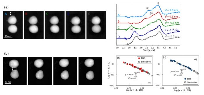
A very unique capability in TEM is the possibility of probing optical properties with sub-nanometre resolution. While light-based methods are the obvious choice for optical characterisation, they are limited to spatial resolutions on the order of tens of nanometres at best. Traditionally, the energy resolution attainable in TEM was insufficient to access the energy ranges relevant for optical excitations. However, continuous advances in instrumentation have bridged this hurdle and improved the energy resolution of state-of-the-art TEMs to values comparable to optical techniques. Another focus of our TEM studies of photonic nanostructures has been metallic nanostructures for plasmonic applications. Plasmonics is an emerging field in which metallic structures are used to guide light or to enhance interactions between light and materials placed in their vicinity. This is due to the ability of these nanostructures to support surface plasmon resonances in the optical range of the electromagnetic spectrum. Our studies have included probing the evolution of the surface plasmon resonances in gold and silver nanoparticles as a function of particle size4 and separation distance between particles5,6, including sub-nanometre separations (Figure 2). The results have provided novel insight into the characteristics of plasmonic nanostructures, otherwise unreachable by optical methods, as well as testing and validating new theoretical descriptions concerned with the plasmonic properties of low dimensional metallic structures7.
Recently, we have expanded the research to include metal alloy nanoparticles showing superior performance for plasmonic ultrafast hydrogen detection8,9.
These examples highlight how improvements in the spatial and energy resolutions of modern TEMs contribute to bridging the gap in our knowledge of the structure – functionality relationship in photonic nanostructures. A step forward in this quest entails in-situ TEM probing of nanostructures under working conditions. In-situ methods in TEM are rapidly expanding, and currently include heating/cooling, electrical biasing, light injection and detection, and gas/liquid environment. Future efforts in this field will focus on combining these tools with TEM measurements of morphology, crystal structure, chemistry, strain, electric field, etc., to “shed better light” on the structure – functionality link in photonic nanostructures.
References
1 S. Kadkhodazadeh, E.S. Semenova, K. Yvind, and R.E. Dunin-Borkowski, J. Cryst. Growth 329, 57 (2011).
2 S. Kadkhodazadeh, E.S. Semenova, M. Schubert, M. Thuvander, K.M. Stiller, K. Yvind, and R.E. Dunin-Borkowski, J. Phys. Conf. Ser. 326, 12046 (2011).
3 D. Cooper, J.-L. Rouviere, A. Béché, S. Kadkhodazadeh, E.S. Semenova, K. Yvind, and R. Dunin-Borkowski, Appl. Phys. Lett. 99, 261911 (2011).
4 S. Raza, S. Kadkhodazadeh, T. Christensen, M. Di Vece, M. Wubs, N.A. Mortensen, and N. Stenger, Nat. Commun. 6, (2015).
5 S. Kadkhodazadeh, J.R. de Lasson, M. Beleggia, H. Kneipp, J.B. Wagner, and K. Kneipp, J. Phys. Chem. C 118, 5478 (2014).
6 S. Kadkhodazadeh, J.B. Wagner, H. Kneipp, and K. Kneipp, Appl. Phys. Lett. 103, 83103 (2013).
7 S. Kadkhodazadeh, T. Christensen, M. Beleggia, N. A. Mortensen, J. B. Wagner, ACS Photonics 4, 251 (2017)
8 S. Kadkhodazadeh, F. A. A. Nugroho, C. Langhammer, M. Beleggia, J. B. Wagner, ACS Photonics 6, 779 (2019)
9 F. A. A. Nugroho, I. Darmadi, L. Cusinato, A. Susarrey-Arce, H. Schreuders, L. J. Bannenberg, A. Bastos da Silva Fanta, S. Kadkhodazadeh, J. B. Wagner, T. J. Antosiewicz, A. Hellman, V. P. Zhdanov, B. Dam, C. Langhammer, Nature Materials 18, 489 (2019)

Researcher Shima Kadkhodazadeh
National Centre for Nano Fabrication and Characterization
DTU Nanolab, Technical University of Denmark
Tel: +45 4525 6494


