
Rositsa Yakimova, of the Department of Physics, Chemistry and Biology (IFM) highlights the strides being made in graphene research
Since the beginning of the new millennium, the properties of graphene stand at the forefront of the fundamental physics and device-oriented research. Although physicists had predicted the unique properties of this material half a century ago, its existence has been questioned or even denied until its demonstration by mechanical exfoliation of highly oriented pyrolytic graphite. Being an electron-rich pi system, graphene possesses unprecedentedly large carrier mobility. This gave promises of tremendous outperforming of the traditional Si-based electronic devices. While graphene physics has enjoyed numerous discoveries made on exfoliated graphene as a unique free-standing 2D material, the demands for practical applications have shifted the focus over the years. Currently, scientists are mainly exploring graphene diversity, including a wide class of low dimensional graphene-related materials (quantum dots, nanoribbons, heterostructures, conductive paints, composites) possessing tunable and narrowly specific properties enabling definite applications. In spite of the increased availability and quality of the varying-sized/shaped graphene, further progress towards electronic components and systems requires integration with different substrates. To this context, epitaxial graphene on SiC that can be formed on semi-insulating (SI) and conductive substrates has appeared on the 2D materials scene as a non-alternative multifunctional product offering a unique complimentary combination of self-assembled graphene layers with a SiC template.
Silicon carbide sublimation
In recent years, the experimental and theoretical studies of Si sublimation from the topmost layers of SiC, and rearrangement of the remaining carbon atoms under specific temperature and pressure settings elucidated the conditions to grow well-ordered epitaxial graphene. During the past decade, Si sublimation technique realised via thermal decomposition of SiC has developed from a facile graphitisation technique to a scale-up production of large-area high-quality monolayer graphene along with the advancements of highly-precise characterisation methods and corresponding theory. A breakthrough was made in 2008 when large area (mm scale) monolayer graphene on SiC was produced, as has been published by the research group at Linköping University (graphene being processed in the laboratory headed by Prof. Rositsa Yakimova). The most outstanding results concerning the epitaxial graphene are related to the demonstration and application of the unique half-integer quantum Hall effect (QHE) with unprecedented robustness and precision (2010). In 2015 for the first time measurements of the QHE with part-per-billion (ppb)-accuracy was demonstrated in a small table-top cryogen-free pulse-tube system. “Both the longitudinal resistivity Rxx and the contact resistance Rc were well within the limits set by the guidelines for primary resistive metrology,” said collaborators from NPL, UK who built up the system [R. Yakimova et al. Operation of graphene quantum Hall resistance standard in a cryogen-free table-top system – 2D Mater. 2 (2015) 035015]. The design and the technical features of the system are easy-to-use and do not require particular experimental skills or laboratory infrastructure, thus significantly advancing production and utilisation of primary quantum standards for precision electrical metrology. Such achievements have been possible only due to the unique properties of the epitaxial graphene on SiC.
Profound studies of graphene on SiC have boosted the discovery of many new physics effects, e.g. magnetic quantum ratchet effect, extremely unusual nature of the carriers, nontrivial magneto-electronic properties, interface-related phenomena, and so on. Furthermore, graphene on SiC allows easy patterning which is used to process, in fact, new materials that is graphene nanoribbons possessing the potential for digital device manufacturing. All these phenomena being graphene on SiC hallmarks are prerequisites for controllable and exclusive manipulation of the graphene/SiC interface towards the design of different high-performance magnetic and electronic devices. In 2011 the first commercial unit in Europe for graphene on SiC production, Graphensic AB was founded by R. Yakimova and co-workers as a spin-off company from LiU, with the aim to link the fundamental research and industrialisation of 2D materials. One of the steps undertaken towards large scale graphene production is the construction of growth equipment for epitaxial graphene on 100 mm SiC wafers and the development of a technological process.
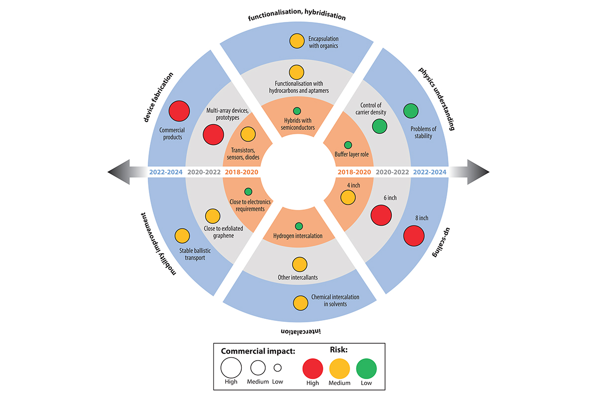
A roadmap for advancement
Despite the large progress that has been made towards graphene globalisation, a roadmap to further advance the epitaxial graphene research is still needed to enable the transition from crude device prototypes to the customer needs. Bearing in mind the already existing concepts and focusing on novel ideas, herein we are proposing a framework for future investigations addressing commercialisation challenges of the epitaxial graphene grown on SiC substrates by their thermal decomposition.
According to our vision efforts should be dedicated to physics understanding, carrier mobility improvement, intercalation, functionalisation, device fabrication, and up-scaling. The roadmap is shown in Fig. 1 covers a 6 year period and includes the mentioned development areas which are expected to have the highest impact on graphene commercialisation. In each area of interest, 3 evolution stages with increasing demands are presumed. The roadmap is also accounting for eventual risk factors which may lead to a time delay from a realistic perspective.
We believe that the knowledge of the state of the art of graphene on SiC should reach the policymakers in Europe and must be considered with a priority in funding distribution for the next 10 years.
Rositsa Yakimova
Department of Physics, Chemistry and Biology (IFM)
Linkoping University
rositsa.yakimova@liu.se
www.ifm.liu.se/materialphysics/semicond
Please note: this is a commercial profile


