Applied nanosciences offer new possibilities for decorative printing and processing, as outlined by Prof. Dr. Silvia Schintke from HEIG-VD-VD/HES-SO Switzerland
With the increasing development of 2D and 3D printing technologies, applied nanosciences, in particular functional nanocomposites and all-solution processing techniques have gained novel economic interest. For example, for industrial applications as transparent electrodes in large area printable electronics and sensor developments, for functionalised surfaces in packaging and security tracking, and also for the field of decorative printing.
R&D at the Laboratory of Applied NanoScience
Main R&D projects at the Laboratory of Applied NanoScience (COMATEC-LANS), of the Department of Industrial Technologies at the HEIG-VD, School of Business and Engineering Vaud of the University of Applied Sciences and Arts Western Switzerland, therefore focus on applied research and demonstrator developments based on nanoparticle inks and nanocomposite materials for 2D and 3D printing and processing technologies, as well as on industrial surface processing techniques and the characterization of nano- and microstructures that are relevant for manufacturing process optimizations or for industrial product and production developments.
In this context, the laboratory COMATEC-LANS/HEIG-VD performs also research on the application of nanoparticle inks, printing and processing technologies for security tags, printable sensors and decorative printing. The engineers and researchers of COMATEC-LANS have elaborated several structuration techniques using printing and processing techniques based on nanoparticle inks and nanocomposite materials. Those are of particular interest for the development of security smart tags and anti-counterfeit applications, e.g. for luxury products or medical products, where the authenticity and traceability of originality are of high relevance. The techniques can furthermore be applied for decorative printing on products or packaging materials.
Printing and applied nanosciences
Results on “Printing and characterizing plasmonic nanoparticles”, “Inkjet-printing of aptamers for printable sensor developments“, as well as on “Atmospheric pressure plasma for patterned inkjet printing and coating on glass” have been presented at international scientific, engineering (IEEE), and industrial conferences and exhibitions of the Printed Electronics (LOPEC), Printing and Glass Industry, and have led to an invited presentation on “Nanocomposite Processing, Coating and Printing Technologies for Smart Packaging and Security Tag Applications” at the World Congress on Smart Materials 2018 in Japan. Part of these recent developments are the outcome of the project NanoInk, an interdisciplinary project at HES-SO, conducted by Prof. Dr. Silvia Schintke within the HES-SO network.
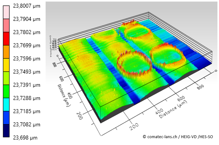
Last but not least, the laboratory COMATEC-LANS of HEIG-VD/HES-SO performs applied research and services for companies, and also trains industrial engineers for the application or implementation of advanced analysis techniques such as non-contact atomic force microscopy, 3D profilometry or optical spectroscopy methods in order to optimise their printing and processing techniques, mastering the nano and micrometre scale of materials and surfaces, as well as their optical, physical-chemical, and electrical performance and surface signatures.
Professor, Head of Laboratory of Applied NanoSciences (COMATEC-LANS)
HEIG-VD, University of Applied Sciences and Arts Western Switzerland (HES-SO)