
Applied nanosciences offer new possibilities for printing and processing, as outlined by Prof. Dr. Silvia Schintke from Heig-VD/HES-SO Switzerland
With the increasing development of 2D and 3D printing technologies, applied nanosciences, in particular functional nanocomposites and all-solution processing techniques have gained novel economic interest. For example, for industrial applications as transparent electrodes in large area printable electronics and sensor developments, for functionalised surfaces in food packaging and security tracking, as well as for the manufacturing of flexible medical electrodes.
Main R&D projects at the Laboratory of Applied NanoScience (COMATEC-LANS), of the Department of Industrial Technologies at the HEIG-VD, School of Business and Engineering Vaud of the University of Applied Sciences and Arts Western Switzerland, therefore focus on applied research and demonstrator developments based on nanocomposite materials for 2D and 3D printing and processing technologies.
Here, we present the impact of applied R&D projects of COMATEC-LANS through 3 show case examples:
Flexible biopolymer nanocomposite electrodes for Medtech applications
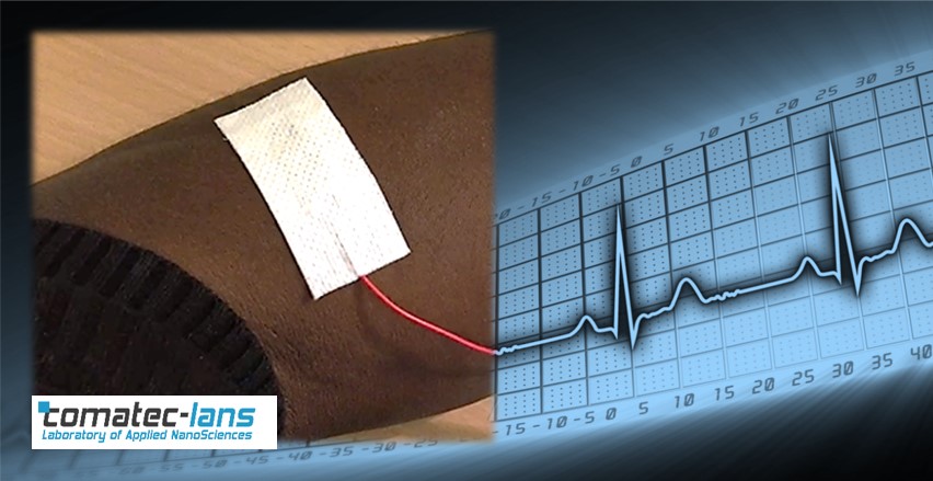
To eliminate the stiff and uncomfortable parts of some of today’s medical electrodes was the aim of an interdisciplinary project involving engineers and scientists from the Laboratory of Applied NanoSciences (COMATEC-LANS) of HEIG-VD and network partners from HES-SO Wallis. The project’s results are highly promising: the novel nanocomposite materials have successfully been tested for medical applications such as signal acquisition in electrocardiograms (ECG), as well as nerf stimulation (TENS). Part of the results have been published recently: in an article “Design and Characterisation of Conductive Biopolymer Nanocomposite Electrodes for Medical Applications” in the journal Materials Science Forum by Trans Tech Publications (2017). Furthermore, various materials processing, printing and coating techniques are applied and developed for nanocomposite polymers at COMATEC-LANS/HEIG-VD.
Hyprid-polymers and nanocomposites for 2D and 3D electrodes and circuits
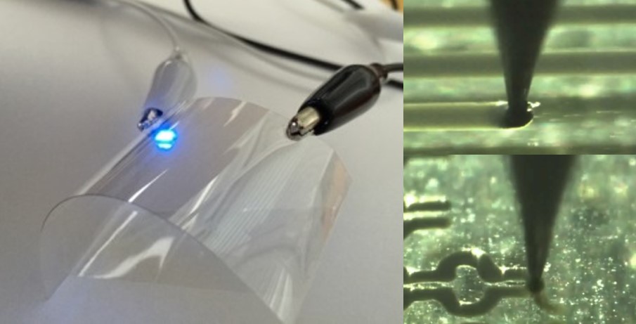
Printable polymer-nanocomposite materials for electrodes and 2D or 3D printable electrical circuits are another R&D focus of the laboratory COMATEC-LANS. One major topic concerns transparent and flexible electrodes; they are in particular of technological relevance in photovoltaic and OLED applications, as well as for flexible displays.
The nano- and micrometerscale topography of oxide based transparent electrodes and of light management structures are studied at COMATEC-LANS/HEIG-VD in joint projects or as a service for companies from the photovoltaic sector. Polymer based transparent electrodes and sensors were e.g. investigated at COMATEC-LANS/HEIG-VD in collaboration with TU Sofia in a project supported by the scientific exchange program Sciex-NMS between Switzerland and the new EU member states. During this project a measurement technique for thin film conductivity of soft materials has been developed, as well as a printable transparent photoelectric sensor.
The developed electrical measurement technique is published in IEEE Xplore (2015) “Electrical characterisation of transparent organic conducting thin films preventing mechanical damage and preserving optical transparency”. Through its design in a transmission line geometry it prevents the soft polymer film to be mechanically damaged by electrical probes and allows for the monitoring of the electrical conductivity under light exposure without probe shadowing effects. The main investigated material was PEDOT: PSS, a transparent hole conductor which is widely used in organic photovoltaics. The influence of various dopants as additives that improve the thin film conductivity and aging behaviour under UV exposure has also been studied in this context.
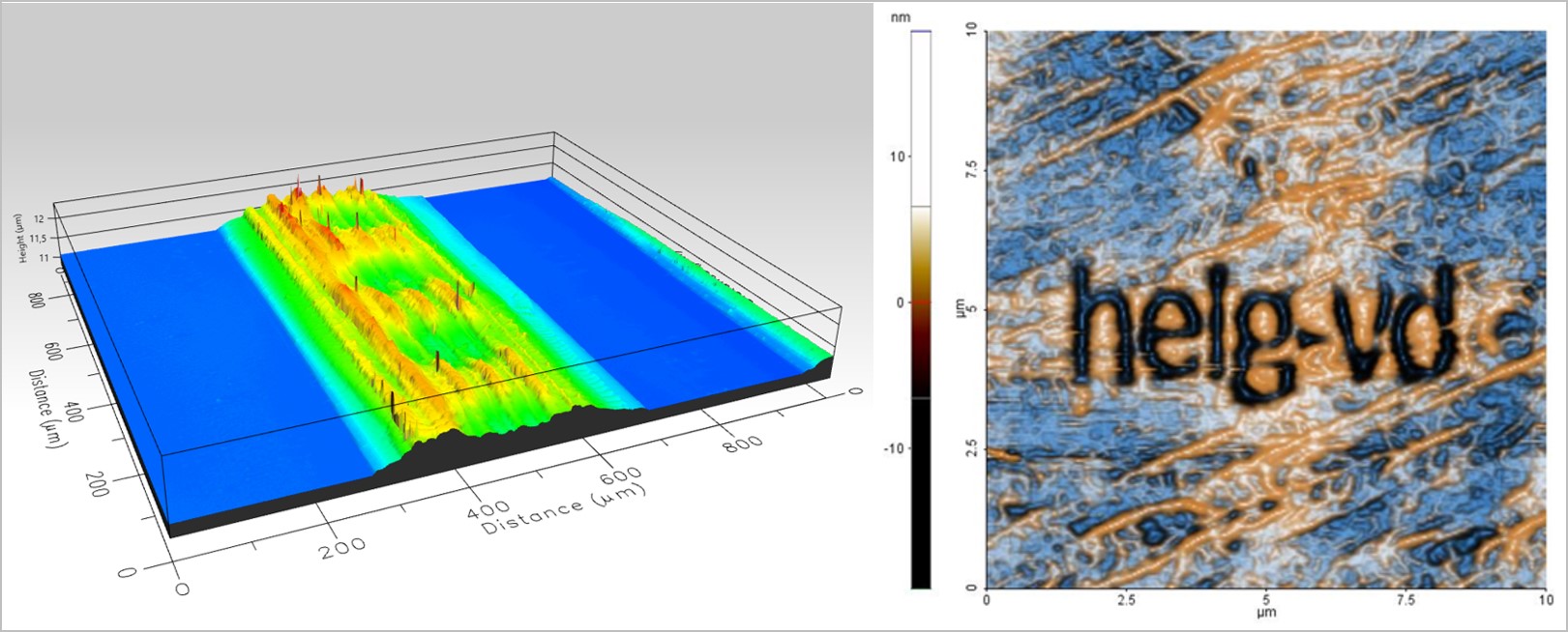
Nano- & microstructures and printing technologies for security tags and printable sensors
Last but not least, the COMATEC-LANS/HEIG-VD performs research and development in the field of printing and processing technologies for surface structuring and functionalisation for security tags and printable sensors. Materials and surfaces are coated or locally functionalised with molecules and/or various nanoparticles and typically studied with advanced non-contact atomic force microscopy techniques, 3D profilometry and optical spectroscopy methods in order to optimise the printing and processing techniques and to analyse advanced security tags at the nano and micrometre scale, as well as for their optical, electrical or magnetic signatures.
Recent results on “Inkjet-printing of aptamers for sensor developments” have been presented at LOPEC, International Exhibition and Conference for the Printed Electronics Industry, 2017. Major collaborative projects of COMATEC-LANS/HEIG-VD in this field concern currently, the surface functionalisation and modifications for the development of sensors and surfaces in biomedical, environmental, food and active or smart packaging applications.
Prof. Dr. Silvia Schintke
Professor, Head of Laboratory of
Applied NanoSciences
HEIG-VD, University of Applied Sciences and Arts Western Switzerland,
silvia.schintke@heig-vd.ch
Please note: this is a commercial profile


