
The Center for Electron Nanoscopy’s Professor Jakob Birkedal Wagner highlights the strides being made in nanoscale imaging research
Following a generous donation from the A. P. Møller and Chastine Mc-Kinney Møller Foundation, the Center for Electron Nanoscopy at the Technical University of Denmark (DTU Cen) was inaugurated in 2007. The center was established as a state-of-the-art electron microscopy (EM) facility with a suite of microscopes housed in a high specification building that only a handful of other labs worldwide could rival. The broad aim of the center is to ensure a balance between advanced research, teaching and training, and fostering collaborations with national and international partners. Now, a decade after the official inauguration of DTU Cen, the center employs 17 researchers (including PhD students and post docs.) as well as 7 technical and administrative staff. Over the years, the activities of the center have been expanding as DTU Cen attracts funding from both Danish and European funding agencies.
Access for academic and industrial scientists to DTU Cen’s electron microscopes supports existing research and results in the creation of new research fields and in the sharing of knowledge for the development of materials, processes, technologies, techniques and instrumentation. The list below gives an idea of the broad research areas that the center is currently pursuing:
- In situ characterization of individual nanoparticles under controlled atmosphere;
- Nanostructures for Plasmonic sensing;
- Magnetic materials;
- Pore structures in minerals and soil;
- (pseudo) 1-dimensional semiconductor heterostructures for solar cells;
- Growth of 1D and 2D carbon structures;
- Grain boundary mapping and phase transitions of alloy materials.
What does EM bring to the table?
Nanotechnology has been a hot topic for more than a decade. The extraordinary properties of materials revealed when structures approach the nanometer regime calls for a better understanding of the structure-functionality relationship. Only by establishing a fundamental understanding of such relationships, is it possible to tailor-make materials and nanostructures for properties not necessarily found in nature.
EM is a versatile tool that can be used to map out the structure and elemental composition of a material from the micrometer scale down to the atomic level. With a spatial resolution in the sub-Ångström regime, it is actually possible to image individual atoms in high-end electron microscopes.
However, even though EM can provide wonderful images of materials at the nano- and micrometer scale, the ultimate goal of EM is not to obtain aesthetically pleasing images, but to advance materials science. This means that EM has to evolve from describing to understanding materials properties.
Considering that that the obtainable resolution in an electron microscope has reached well below 0.1 nm, the challenge now lies with improving time resolution with high sensitivity. Game-changing developments in high-speed cameras and highly sensitive detectors are creating the platform for making EM an even better analysis tool, especially in so-called in situ EM studies in which the electron microscope is used as an in situ experimental laboratory. The analysis of the dynamical response to stimuli such as heat, gas and liquid exposure, electrical bias, stress, illumination, magnetic fields, etc. are all possible by using in situ EM.
Even though EM is a powerful tool for studying materials it should not be seen as a stand-alone technique, but has to be used in a complementary way with other methods. Furthermore, high-end electron microscopes are usually very specialized in order to push the limits. Thus, a centralized infrastructure like DTU Cen with a broad suite of electron microscopes and the accompanying expertise is more beneficial than having single instruments spread over a wide area. You could consider high-end EM as Formula One; you need a good car (microscope), a good driver (operator/scientist) and a comprehensive support team (technician, materials science collaborators) to achieve outstanding results. If one is missing, you have to settle for the mediocre.
Highlights from DTU Cen
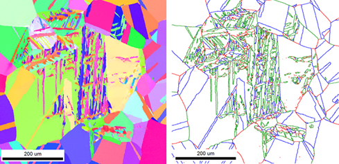
The mechanical properties of materials are strongly related to grain size, grain boundary length and type. Mapping the microstructure in terms of phase and orientation in the way shown in Figure 1 before, after and (ideally) during mechanical treatment or annealing, provides invaluable insight into the relationship between macroscopic mechanical properties and the microstructure. Such insight and fundamental understanding are aids towards creating tailor-made materials for wind-turbines, aircraft parts and other materials used in harsh environments.
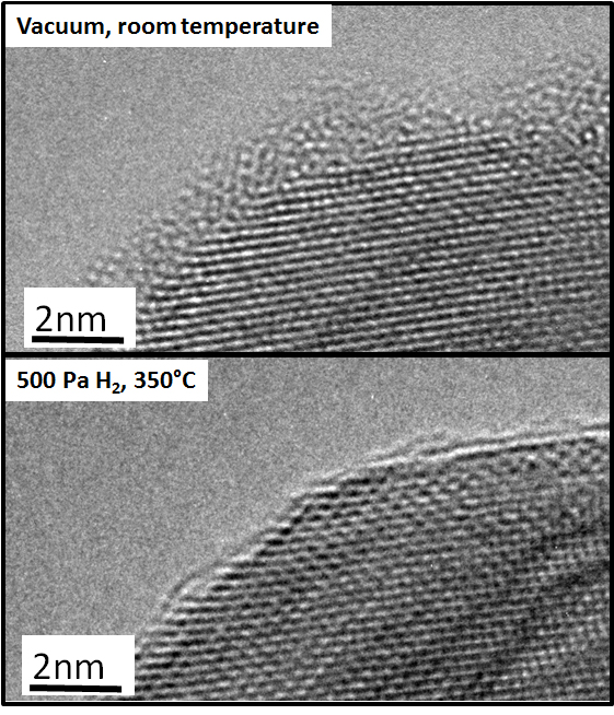
Chemical surface reactions, such as those taking place in catalytic processes, are highly dependent on the atomic structure of the active species. The structural aspects of the materials often change with the environment (gas, temperature, etc.). This means that in situ studies are necessary to obtain the real picture of the active material. In Figure 2, a Pd surface is viewed as synthesized and during reduction in hydrogen at elevated temperature. The native oxide layer of the particle is removed and the relevant structure of the surface is revealed.
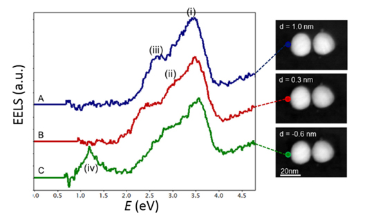
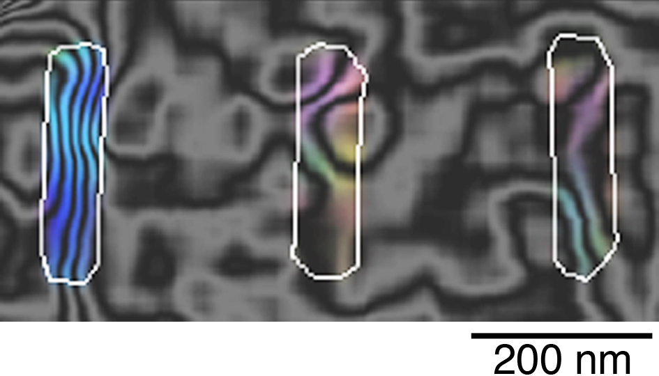
EM also provides the possibility to map out plasmonic responses via electron energy-loss spectroscopy and magnetic fields by electron holography. Figure 3 shows an example of the spatially resolved plasmonic response probed by swift electrons of gold and silver. Electron holography allows magnetic and electric fields in materials to be studied quantitatively at the nanometer scale. Figure 4 shows in-situ magnetic reversal behaviors of individual pseudo-spin-valve thin-film elements (NiFe/ Cu/Co) after the application of a magnetic field, suggesting a variation of the switching field in the adjacent elements.
Professor Jakob Birkedal Wagner
Scientific Director, Center for Electron Nanoscopy
DTU Cen, Technical University of Denmark
jakob.wagner@cen.dtu.dk
Please note: this is a commercial profile


