
Dr Dimiter Prodanov from Imec explains the guiding principles in technological development of novel nanomaterials
Nanomaterials are fascinating for the wide variety of their unique properties, which can be used to improve everyday life. Such desirable characteristics can include the increased strength of the nano-enabled material, its chemical reactivity or altered electrical properties. Deliberately designed, that is, engineered nanomaterials (ENM) are used in a wide variety of applications, from cosmetics and paints to sportswear and semiconductor chips. Use of ENM rests at the core of modern nanotechnology.
Top-down and bottom-up approaches to nanotechnology
From a technological perspective, there are two complementary approaches to nanotechnologies: a top-down and a bottom-up manufacturing. While the bottom-up approach can be broadly identified as nanoparticle synthesis or self-assembly; the top-down approach consists of growth or deposition on surfaces often in combination with nano-patterning techniques. An example of the latter is in the nano-electronics industry. In the broad sense, end-user nanomaterial industries are also nanotechnological since they incorporate engineered nanomaterials into macroscopic objects.
The precautionary principle advises that some ENM may have enhanced or altered toxicity compared to their bulk counterparts. Examples here are various nanofibers or photocatalytic nanoparticles. While for chemicals there are established regulatory frameworks dealing with the potential risks to consumers, workers and the environment, this is not the case for nanomaterials. Safe-by-design approaches in nanotechnology are, therefore, increasingly being explored by regulators and policymakers in Europe. While in mature industries, such as in construction, these can easily be decoded into specific engineering requirements for the construction of buildings or bridges, the safe-by-design concept for nanomaterial synthesis, representing bottom-up nanotechnology, remains somehow abstract. It could be, therefore, be useful to transfer experience from other, more technologically mature sectors, such as integrated circuit manufacturing.
The technologies used in nanoelectronics offer an unprecedented control of the properties of the finished product at an affordable cost and high yield of the finished devices. To do so, the nanoelectronics industry introduces a variety of novel materials, which are used at the nanoscale level. Typically, the product development runs ahead of establishing precise limits for the occupational and environmental hazards of these materials. Since nanoelectronics research and development (R&D) deals with novel materials and processes, the challenge is the lack of information leading to uncertainty in risk grouping and governance.
NanoStreeM to set up the nano-safety roadmap in semiconductor R&D
Since 2016, the NanoStreeM project1 has developed a framework for a safety assessment of new nanostructured materials, for example, quantum dots, different types of nanofibers, or 2D materials, such as nanosheets like graphene. By performing an extensive literature review, the team of Dr Michael Jank from the Fraunhofer Institute for Integrated Systems in Erlangen, together with colleagues from IMEC, Belgium, have established some guiding principles in technological development. These can be summarised as follows:
Lab-scale research typically employs the direct handling of ENM in a bottom-up manner, which can pose occupational but not consumer or environmental hazards. This is because the deployed technologies are of low maturity (that is not present in finished products) and small scale.
As the technology becomes more mature, the yield requirements lead to innovations that favour precisely aligned and reproducible placement and, therefore, avoid direct handling of ENM. Workers are not likely to get exposed since processing favours closed systems. At this stage, free nanomaterials may be present during some processing stages, but the consumer is not directly exposed to them during the intended use of the finished product.
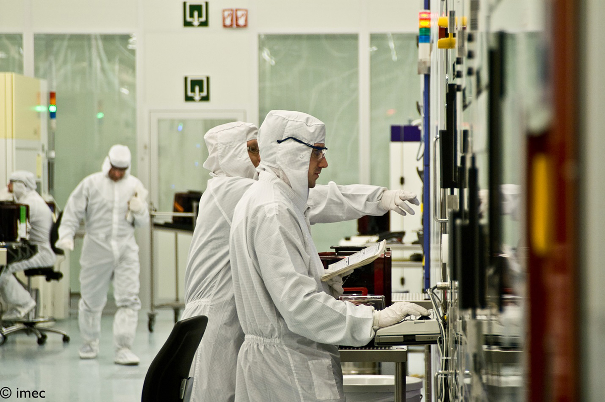
Finally, mature technologies for ultra-large-scale integration (ULSI, see photo above) because of their performance and yield requirements, lead to the deployment of approaches, which are compatible with the present planar technologies, based on silicon and germanium. That is, nanostructures are patterned in a top-down manner which avoids direct exposure to the ENM and, therefore, reduces both occupational and consumer exposure. Therefore, top-down fabrication of nano-functionalised materials and devices is unlikely to add unanticipated hazards only because used materials are “nano”.
The results of the study have been discussed by an expert panel held at a satellite workshop at Semicon Europa, Munich on 14 Nov 2018 (see photo). The panel agreed that the R&D approach in semiconductor industry represents an example of the safe-by-design approach that may have some generic properties transferable to other industries. Furthermore, the existing European regulatory risk assessment approach, represented by the REACH Regulation 1907/2006 and the Chemical Agents Directive, in combination with the ISO Standard ISO/TS 12901-2:2014 can also be suitably used for the novel materials deployed by the semiconductor R&D. However, more attention is needed in assessing possible environmental hazards at the end-of-life of different products and the possibilities for recycling of rare elements. The full workshop report is available on the NanoStreeM website.
1 The NanoStreeM project (Nanomaterials: strategies for safety assessments in advanced integrated circuits manufacturing) receives funding from the European Union’s Horizon 2020 Research and Innovation Programme under grant agreement n° 688794.
Please note: this is a commercial profile
Dr Dimiter Prodanov
IMEC vzw
Tel: +32 162 818 40


