
Alice Bastos da Silva Fanta, senior researcher at the Center for Electron Nanoscopy explores the world of Transmission Kikuchi diffraction (TKD) in the scanning electron microscope (SEM), a technique, she argues, that came to stay
The microstructure and composition of a material influences its properties and consequently, its applications. At the same time, the microstructure of a material is influenced by the fabrication method and process. Furthermore, it can change during operation, due to, for example, environment or process changes. New technology development needs to be in close relationship with microstructure characterisation and understanding. Numerous techniques to study materials microstructure and composition exist and in general, only the combination of them enables the required understanding of the microstructure.
One technique commonly applied when characterising crystalline materials is electron backscatter diffraction (EBSD), which is an electron microscopy technique used to obtain quantitative information from crystalline samples in a scanning electron microscope (SEM). The diffraction patterns backscattered from small volumes close to the surface of a flat sample are automatically indexed as the electron beam scans the sample. The characteristic diffraction patterns allow for a reconstructed crystal orientation map of the sample. EBSD is a powerful technique to study size, shape and distribution of grains and grain boundaries, in addition to local crystal orientation and misorientation of the sample. It can be combined with other techniques, such as energy dispersive X-ray spectroscopy (EDS) for elemental analysis, or a focused ion beam and is widely used in many research fields and industries to characterise microstructure and texture.
Although EBSD is applied extensively for linking process, structure and properties of materials and minerals, its spatial resolution is insufficient to truly characterise nanoscale materials. This class of materials has been traditionally investigated using transmission electron microscopes (TEMs). However, thanks to the recent work of Keller and Geiss1, an alternative way of studying electron transparent samples with an EBSD detector was proposed and the application of EBSD could be extended to nanocrystalline materials. Although this new approach was first called t-EBSD (for transmission EBSD), it is now known as transmission Kikuchi diffraction (TKD).
The improvements in spatial resolution make it comparable with diffraction mapping techniques in the TEM. Considering the flexibility, the accessibility and the relatively simpler operation of a SEM in comparison to TEM, TKD has potential to become as widely applied in nanocrystalline material characterisation. Furthermore, as SEM operates at lower energy ranges than TEM, TKD can be an alternative technique to explore and investigate electron beam sensitive crystalline materials.
At DTU Cen, we focus on developing, exploring and applying TKD to correlate microstructure with properties of low dimensional nanocrystalline materials. In this light, we study nanowires, nanoparticles and thin films with TKD2–5, optimising sampling conditions6, performing dynamic experiments7 and improving detection capabilities.
Solid-state dewetting is a phenomenon in which a continuous film agglomerate at elevated temperature forming particles. The importance of understanding the microstructure features influencing this process is two-fold: firstly, avoiding the film breakdown during device operation is essential to ensure functionalities, and secondly, this phenomenon can be employed as an effective tool for fabricating ordered nanoparticle arrays which find applications in, for example, optical devices. Figure 1 (a) shows a series of TKD maps revealing a gold film of 20 nm starts dewetting already at temperatures below 200°C, under 50 Pa water pressure7. Such temperatures are easily achieved during device fabrication and operation. Changing the environment, or adding an adhesion layer, influences the extent of dewetting, as shown in Figure 1(b). A fundamental understanding of the starting point of the dewetting process is essential in order to predict and control the microstructure to avoid dewetting, or to tailor the dewetting depending on the application of interest.
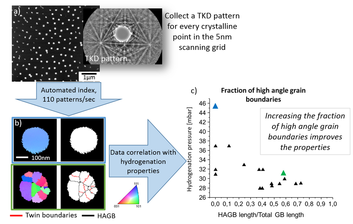
TKD investigation of palladium nanoparticles used in hydrogen sensing devices, reveals that particle microstructure is significant for the hydrogenation and dehydrogenation properties. The correlation of the quantitative data obtained by TKD with the single particle plasmonic response allows us to distinguish the key microstructural feature influencing the hydride formation and decomposition which is directly related to the hydrogen sensing properties of the nanoparticles (Fig. 2)4. The fundamental understanding of the microstructure and its role on the particle properties enables the control and design of improved hydrogen sensors; essential for developing a hydrogen economy, since hydrogen is highly flammable in air, and for safety reasons, any leaks must be immediately detected.
These examples highlight the potential of TKD for nanoscale characterisation and for studying structure – functionality relationship. The methodology applied to these examples is well suited for many other systems and platforms and it can be predicted that it will be widely employed in the near future. Since the TKD technique is relatively new, it is natural that there is room for improvements, therefore, our future efforts in the field will focus on improving detection capability to enlarge and improve the application field of the technique.
References
1 Keller, R. R.; Geiss, R. H. Transmission EBSD from 10 Nm Domains in a Scanning Electron Microscope. J. Microsc. 2012, 245 (3), 245–251.
2 Todeschini, M.; Bastos Da Silva Fanta, A.; Jensen, F.; Wagner, J. B.; Han, A. Influence of Ti and Cr Adhesion Layers on Ultrathin Au Films. ACS Appl. Mater. Interfaces 2017, 9 (42).
3 Wickman, B.; Bastos Fanta, A.; Burrows, A.; Hellman, A.; Wagner, J. B.; Iandolo, B. Iron Oxide Films Prepared by Rapid Thermal
Processing for Solar Energy Conversion. Sci. Rep. 2017, 7, 40500.
4 Alekseeva, S.; Fanta, A. B. da S.; Iandolo, B.; Antosiewicz, T. J.;
Nugroho, F. A. A.; Wagner, J. B.; Burrows, A.; Zhdanov, V. P.;
Langhammer, C. Grain Boundary Mediated Hydriding Phase Transformations in Individual Polycrystalline Metal Nanoparticles. Nat. Commun. 2017, 8 (1), 1084.
5 Zhu, X.; Todeschini, M.; Bastos da Silva Fanta, A.; Liu, L.; Jensen, F.; Hübner, J.; Jansen, H.; Han, A.; Shi, P.; Ming, A.; et al. In-Depth Evolution of Chemical States and Sub-10-Nm-Resolution
Crystal Orientation Mapping of Nanograins in Ti(5 nm)/Au(20 nm)/Cr(3 Nm) Tri-Layer Thin Films. Appl. Surf. Sci. 2018, 453, 365–372.
6 Niessen, F.; Burrows, A.; Fanta, A. B. da S. A Systematic Comparison of on-Axis and off-Axis Transmission Kikuchi Diffraction. Ultramicroscopy 2018, 186, 158–170.
7 Fanta, A. B.; Todeschini, M.; Burrows, A.; Jansen, H.; Damsgaard, C. D.; Alimadadi, H.; Wagner, J. B. Elevated Temperature Transmission Kikuchi Diffraction in the SEM. Mater. Charact. 2018, 139, 452–462.
Please note: this is a commercial profile
Alice Bastos da Silva Fanta
Senior researcher
Center for Electron Nanoscopy
Tel: +45 4525 6469


