
Here, Alice Bastos da Silva Fanta, discusses the long-lasting use of Transmission Kikuchi diffraction (TKD) in the SEM
The microstructure and composition of a material influence its properties, and consequently its applications. Controlling such relationships by fabrication methods and process allow for materials with tailored properties. Numerous techniques to study materials microstructure and composition exist and in general, only the combination of them enables the required understanding of the microstructure.
Electron backscatter diffraction (EBSD)
Electron backscatter diffraction (EBSD) is commonly applied when characterising crystalline materials to obtain quantitative information from crystalline samples in a scanning electron microscope (SEM). The diffraction patterns backscattered from small volumes close to the surface of a flat sample, are automatically indexed as the electron beam scans the sample in order to construct a crystal orientation map of the sample. EBSD is a powerful technique to study size, shape and distribution of grains and grain boundaries in addition to local crystal orientation and misorientation of the sample. Combined with other techniques, such as energy dispersive X-ray spectroscopy (EDS) for elemental analysis, or a focused ion beam makes it widely used in many research fields and industries to characterise microstructure and texture.
Transmission Kikuchi diffraction (TKD)
At DTU Nanolab, we focus on developing, exploring and applying TKD to correlate microstructure with properties of low dimensional nanocrystalline materials. One example is to take advantage of the thin sample to simultaneously acquire STEM images and Kikuchi patterns. This makes direct comparison of the morphology and crystalline structure of the material during in situ treatment at elevated temperature possible.2 In this light we study nanowires, nanoparticles and thin films with TKD3–6, optimising sampling conditions7, performing dynamic experiments8 and improving detection capabilities2.
Solid state dewetting is a phenomenon in which a continuous film agglomerate at elevated temperature forming particles. The importance of understanding the microstructure features influencing this process is two-fold: First avoiding the film breakdown during device operation is essential to ensure functionalities, and second, this phenomenon can be employed as an effective tool for fabricating ordered nanoparticle arrays, which find applications in, for example, optical devices. Figure 1 (a) shows SEM images and orientation maps of a gold film of 20nm starts at room temperature and 250°C revealing structural changes at elevated temperature. A fundamental understanding of the starting point of the dewetting process is essential in order to predict and control the microstructure to avoid dewetting or to tailor the dewetting depending on the application of interest.
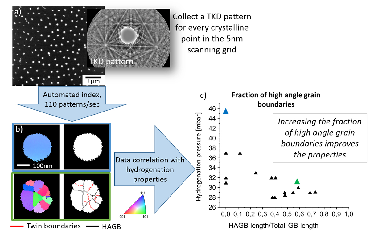
TKD investigation of palladium nanoparticles used in hydrogen sensing devices, reveals that the particle microstructure is significant for the hydrogenation and de-hydrogenation properties. The correlation of the quantitative data obtained by TKD with the single particle plasmonic response allows to distinguish the key microstructural feature influencing the hydride formation and decomposition which is directly related to the hydrogen sensing properties of the nanoparticles (Fig. 2)5. The fundamental understanding of the microstructure and its role on the particle properties enables the control and design of improved hydrogen sensors; essential for developing a hydrogen economy, since hydrogen is highly flammable in air, and for safety reasons, any leaks must be immediately detected.
These examples highlight the potential of TKD for nanoscale characterisation and for studying structure – functionality relationship. The methodology applied on these examples is well suited for many other systems and platforms and it can be predicted that it will be widely employed in the near future. Since the TKD technique is relatively new, it is natural that there is room for improvements, therefore our future efforts in the field will focus on improving detection capability to enlarge and improve the application field of the technique.
Please note: This is a commercial profile
(1) Keller, R. R.; Geiss, R. H. Transmission EBSD from 10 Nm Domains in a Scanning Electron Microscope. J. Microsc. 2012, 245 (3), 245–251.
(2) Fanta, A. B.; Fuller, A.; Alimadadi, H.; Todeschini, M.; Goran, D.; Burrows, A. Improving the imaging capability of an on-axis transmission Kikuchi detector. Ultramicroscopy 2019, 206, 112812
(3) Todeschini, M.; Bastos Da Silva Fanta, A.; Jensen, F.; Wagner, J. B.; Han, A. Influence of Ti and Cr Adhesion Layers on Ultrathin Au Films. ACS Appl. Mater. Interfaces 2017, 9 (42).
(4) Wickman, B.; Bastos Fanta, A.; Burrows, A.; Hellman, A.; Wagner, J. B.; Iandolo, B. Iron Oxide Films Prepared by Rapid Thermal Processing for Solar Energy Conversion. Sci. Rep. 2017, 7, 40500.
(5) Alekseeva, S.; Fanta, A. B. da S.; Iandolo, B.; Antosiewicz, T. J.; Nugroho, F. A. A.; Wagner, J. B.; Burrows, A.; Zhdanov, V. P.; Langhammer, C. Grain Boundary Mediated Hydriding Phase Transformations in Individual Polycrystalline Metal Nanoparticles. Nat. Commun. 2017, 8 (1), 1084.
(6) Zhu, X.; Todeschini, M.; Bastos da Silva Fanta, A.; Liu, L.; Jensen, F.; Hübner, J.; Jansen, H.; Han, A.; Shi, P.; Ming, A.; et al. In-Depth Evolution of Chemical States and Sub-10-Nm-Resolution Crystal Orientation Mapping of Nanograins in Ti(5 nm)/Au(20 nm)/Cr(3 Nm) Tri-Layer Thin Films. Appl. Surf. Sci. 2018, 453, 365–372.
(7) Niessen, F.; Burrows, A.; Fanta, A. B. da S. A Systematic Comparison of on-Axis and off-Axis Transmission Kikuchi Diffraction. Ultramicroscopy 2018, 186, 158–170.
(8) Fanta, A. B.; Todeschini, M.; Burrows, A.; Jansen, H.; Damsgaard, C. D.; Alimadadi, H.; Wagner, J. B. Elevated Temperature Transmission Kikuchi Diffraction in the SEM. Mater. Charact. 2018, 139, 452–462.


