
Nanoscale fabrication and nanoscale characterisation when it comes to materials are placed under the spotlight here by Professor Jakob Birkedal Wagner, Head of Nanocharacterization Section at DTU Nanolab, Technical University of Denmark
Nanoscale fabrication and nanoscale characterisation are entangled to a large degree. Nanofabrication allows for synthesis and formation of tailor-made materials and structures with properties not necessarily found naturally on Earth, bringing value to the society in terms of higher energy efficiency, higher sustainability, increased living standards via advanced tools for medical treatment to name a few.
The fabrication or synthesis of nanostructured materials relies on top-down or bottom-up processes. In order to gain control of such processes, the individual steps have to be closely monitored.
The National Centre for Nano Fabrication and Characterization at the Technical University of Denmark (DTU Nanolab) embraces both the state-of-the-art fabrication of micro- and nanostructures, as well as characterisation of said structures by means of the state-of-the-art electron beam based microscopy and spectroscopy helping to bring the fundamental research into applications.
DTU Nanolab operates and maintains advanced processing equipment within 1350 m2, class 10-100, ISO 9001-certified, open access, pay-per-use cleanroom facilities. In a separate specially constructed building, the centre operates eight state-of-the-art electron microscopes, among them four Transmission Electron Microscopes (TEM) and a Dual Beam Scanning Electron Microscope (FIB-SEM).
The fabrication part of DTU Nanolab is built as a versatile micro- and nanofabrication platform in order to shape a wide range of materials with structures down below 20 nanometers on substrates up to 8” in size. This includes a comprehensive and expanding selection of state-of-the-art process equipment for lithography, etching, thermal processing, thin film deposition, wafer cleaning, advanced packaging and characterisation.
The characterisation part of DTU Nanolab has established world-class expertise within material characterisation. Our state-of-the-art equipment allows for high spatial resolution imaging and spectroscopy at elevated temperature in gaseous environments.
The combined facility has currently around 100 staff members and over 450 registered users, active in research, education, analysis, material characterisation, development, prototyping and small-scale production. DTU Nanolab’s scientific staff are pushing the state-of-the-art in characterisation and fabrication by conducting research on new electron beam based microscope techniques and new micro- and nanofabrication technologies. Engineers and technicians repair and maintain the equipment, train and help the various users to achieve their respective goals.
DTU Nanolab is located on DTU’s main campus in Lyngby, 15 km north of the centre of Copenhagen, Denmark around 30 minutes from Copenhagen Airport Kastrup.
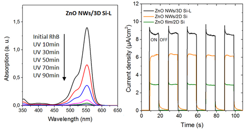
The integration of low-dimensional nanomaterials with hierarchical three-dimensional microstructures opens up the possibility for the realisation of novel properties or improved functionalities. Figure 1 shows an example of such integrated structures. Heavily doped silicon has been fabricated into a highly-ordered 3D micro-mesh structures by standard photolithography, followed by a modified plasma etch process.1 The density of the integrated ZnO nanowires (NWs) into the mesh is increased by approximately an order of magnitude in comparison with a more traditional 2D substrate. The performance of photocatalytic degradation and photocurrent generation (Figure 2) scales with the ZnO NW density.
Application of gold thin films within plasmonics, metamaterials, 2D materials and nanoelectronics, relies on efficient adhesion of gold layers on dielectric or semiconductor substrates. Downscaling in nanoscience and technology brings the dimensions of thin metal layers to be similar to adhesion layer implying a strong structured relationship to be explored for efficient application.
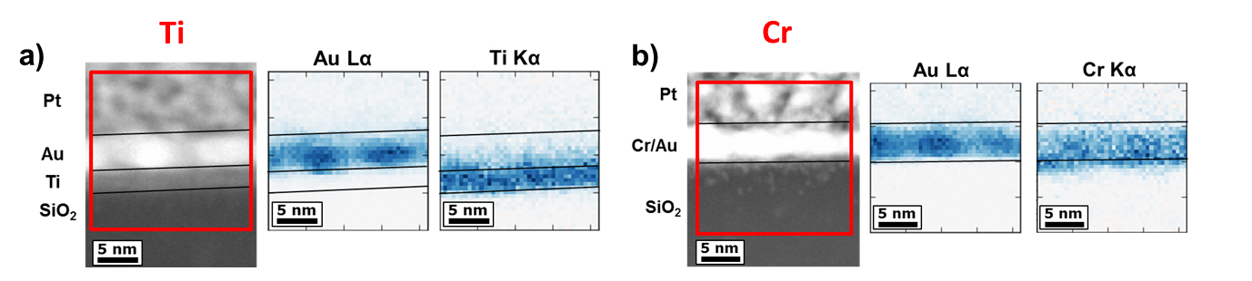
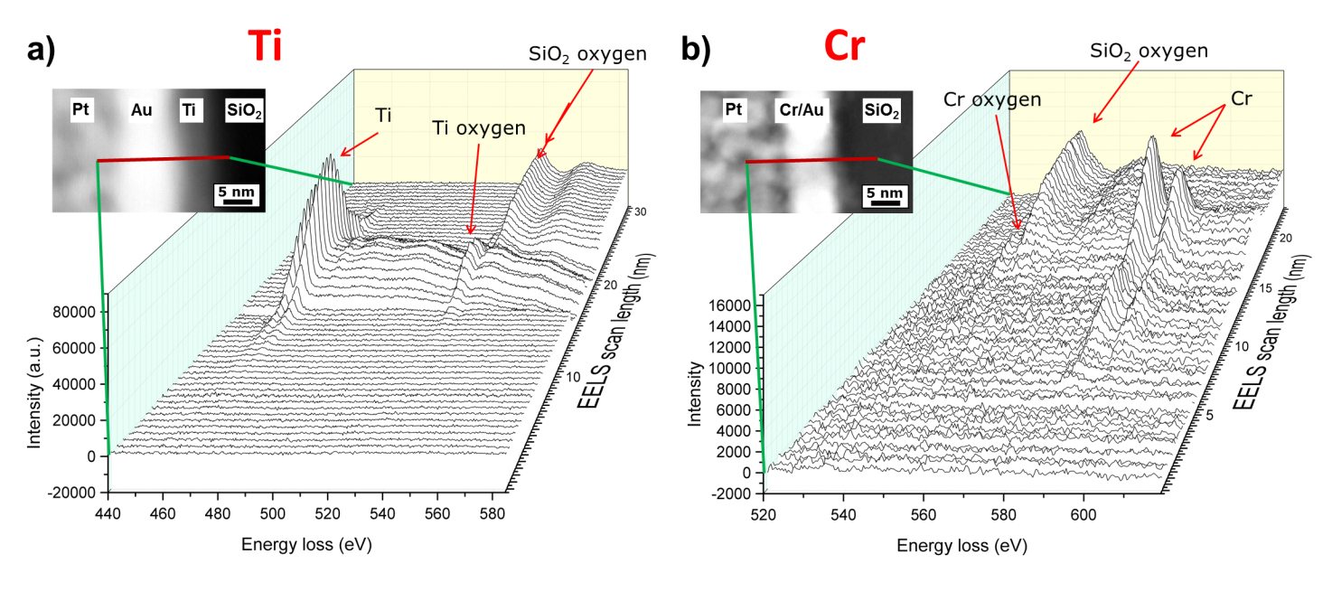
Fabrication of such layered structures by e-beam evaporation and close monitoring by means of characterisation at the sub-nanometer scale brings a better understanding of the interdiffusion, as well as the structural behaviour of the evaporated layers2 (Fig. 3 and 4).
Please note: this is a commercial profile
References
1 B. D. Chang et al., ChemNanoMat 2018, (4), doi: 10.1002/cnma.201800371, Highly Ordered 3D Silicon Micro-Mesh Structures Integrated with Nanowire Arrays: A Multifunctional Platform for Photodegradation, Photocurrent Generation, and Materials Conversion’.
2 M. Todeschini et al., ACS Applied Materials & Interfaces 2017, (9), 37374, ‘Influence of Ti and Cr Adhesion Layers on Ultrathin Au Films’.
Professor Jakob Birkedal Wagner
Head of Nanocharacterization Section
DTU Nanolab,
Technical University of Denmark
Tel: +45 4525 6471
jakob.wagner@cen.dtu.dk
www.cen.dtu.dk
www.danchip.dtu.dk


