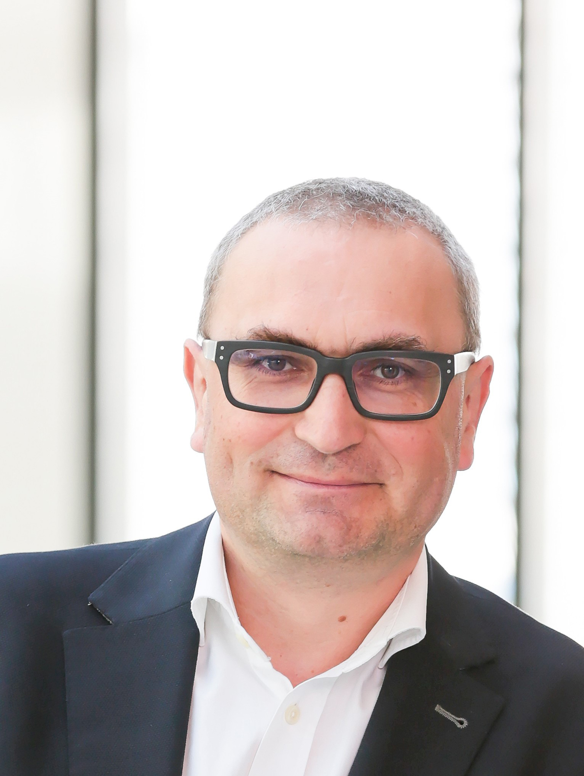
Toralf Scharf, Senior Scientist/Faculty member at ÉCOLE POLYTECHNIQUE FÉDÉRALE DE LAUSANNE EPFL explains the challenges present in modern optical technologies
In the 21st century, optical technologies start to gather fruits for its long investment in research and development supported by technologies developed for microelectronics. The basic driver is miniaturisation and with the maturity of micro- and nanofabrication tools even standard optical components like lenses will change their appearance. Especially the move from single components, to complete systems and their integral optimisation will challenge the research and development activities and opens a disruptive pathway to optical component design and manufacture. Everything gets smaller, everything must interact perfectly, and everything should be designed together.
While in former times of technology development, the global players run own research labs and opted for widespread dissemination of knowledge through publications today, the situation is different. The technology drivers keep their activity secret and additionally outsource the technology – by taking care that their developments are not transferred to other projects within the same lab and putting effort into patenting.
The technology development has undergone a fundamental change from an open culture to a more restricted one! One additional aspect is that many innovative developments today come from small enterprises or start-ups before they are transferred to global operators. Such small and medium-sized companies have a completely different strategy for sharing results. It is mainly done based on new products and fabrication secrets. Patents are only important if venture capital is involved.
Moreover, because of limited resources, SMEs are calling often for public research funds and immediately get a conflict of interest: it is important to make results available with open access, as asked for by the funding agencies and keeping fabrication secrets as needed for the running of the business. The push towards open access will nevertheless help SMEs – as they have only limited resources for research and can profit much more from wider dissemination of results – because SMEs are more dynamic to adapt.
At the same time, in our highly specialised technology-driven world top-level research becomes even more expensive. This is mainly due to fact that enterprises specialised in their field invest enormous amounts of money in production facilities and machines to keep the lead in their field. On the other hand, research funds at Universities are limited and with the trend to common technological platforms, more standard equipment will be used but made available to the wider community.
A technological and educational gap appears and makes it very difficult to educate engineers with cutting-edge techniques, or to contribute to latest high technology development in research. This is also valid for optics fabrication that covers an enormous span of different technology, from grinding and polishing to electron beam writing. One solution here is to establish close collaboration with industry and install industrial PhD programmes.
If we look at technologies, what are the ongoing challenges? As mentioned optics uses many different techniques but with the same goal: achieving the optical quality of the components. The term “optical quality” stands for nanometre precision. For lenses, it means excellent surface definition and quality, but for nanostructured components, its definition becomes more complex and includes uniformity over surfaces of millimetre size. If we look at miniaturisation in optics, we see several challenges.
Firstly, the optical elements need to be connected to the macroscopic world and will need to cover a certain surface or volume. High-quality production over millimetres for nanometre scale structures needs to be developed.
Secondly, to fully profit from the fine structure of the components one would like to change parameters of nanostructures locally. With mm size optical element and a 100 nm sized basic structural element, one ends up with more than 100 million elements. If only a few of them are used for the design of an optical function, then the parameters space for optimisation will not be manageable with conventional design approaches. An optical multidimensional system design can handle many parameters and is based on a rigorous method which needs to become the standard. An optical design will become a big data problem.
A third challenge is the characterisation at different lengths of scale. Often underestimated, is the link between the quality of nanostructures and its optical function which is not easy to establish. The ultimate characterisation technique would have a large field of view in the millimetre range – to see the whole element at once and still deliver nanometre resolution. But such techniques do not exist yet and would lead to data volumes for analyses that are not manageable by the existing informatics infrastructure. The optical characterisation is already a big problem where data is concerned.
With all these different aspects in mind, what is the ideal research project to educate future engineers and scientists? We found an answer in a project that is based on industrial collaboration including all aspect of optical technology. Our activities are based on experiences in the most modern fields of research in optics: nano-photonics including meta-surfaces and meta-materials, micro-optics referring to refractive and diffractive structures and system optics which takes up the different aspects of integrating such components.
The EU funded Horizon 2020 research project NOLOSS allows 15 fellows to pursue their PhDs in the industry in the framework of a European Industrial Doctorate (EID) Marie Curie Actions. With 12 participants, including nine partners from the industry, this allows us to widen the view of technology development at industrial partners, as they expand their network to SMEs that would not otherwise be possible. Of course, this needs learning and support from all sides.
The funding agencies need to be aware that industries of different sizes work at different pace and need to change direction to keep on track with their business. The universities must understand that a PhD outside of their infrastructure will contribute differently to the universities communities and the fellows must be flexible to accept different workplaces during their studies.
But all this can be managed and the NOLOSS project is an excellent example how it can be done on a scale needed to develop an effective network and to have the most important technologies on board. This said, keeping an open science attitude is not easy and the push for publications and dissemination remains one of the greatest challenges of the project.
Toralf Scharf focuses his research activities at the École polytechnique fédérale de Lausanne on interdisciplinary subjects bringing micro-system, material technology and optics together. With a background in surface physics (MSc), physical chemistry (PhD) and a profound experience in optics he is familiar with all necessary aspects of technology development and application and can communicate with different scientific communities. In over 20 years of project execution with industry and governmental organisations, he has accumulated the right experience to lead and execute the project at different levels.
Funding
This project has received funding from the European Union’s Horizon 2020 research and innovation programme under the Marie Sklodowska-Curie grant agreement No 675745.
Website https://www.nolossproject.eu
Please note: this is a commercial profile

Toralf Scharf
Senior Scientist/Faculty member
ÉCOLE POLYTECHNIQUE FÉDÉRALE
DE LAUSANNE EPFL
Tel: +41 21 695 4286


