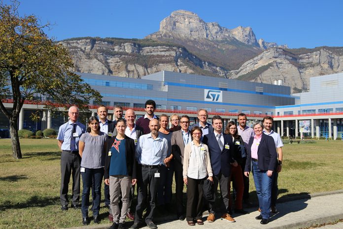
Dimiter Prodanov from Imec and Daniela Iacopino from Tyndall reveal how NanoStreeM has set up the nano-safety roadmap when it comes to semiconductor research and development
The semiconductor industry uses a growing variety of materials, as companies seek to further improve devices’ performance to meet increasing market demand in a constant process of innovation. At present, there are more than 200 chemical compounds consisting of elements, such as silicon, germanium, copper, gold, hafnium, indium and many others, which are present in most computer and mobile phone chips. Understanding the properties of these innovative materials and nanoforms, and how they behave in living systems, such as the human body, often comes years after the materials have been introduced in manufacturing. Such an inherent uncertainty brings about multiple challenges in the governance of the occupational and environmental risks. This is a common challenge for many technology-intensive sectors and it requires a systematic risk reduction approach. This understanding was the driving force behind the NanoStreeM project, which was funded by the European Union (EU) from 2016 until 2018. The objectives of the project were to:
- Build inventories of materials, research topics and applications relevant for nanomaterial use and exposure in nano-electronics manufacturing;
- Identify gaps in knowledge and methodologies to assess the risk of engineered or accidentally produced nanomaterials and;
- To inform stakeholders in order to support decision making and governance of the risks related to the use of nanomaterials and nanoforms in the semiconductor fabrication process.
The NanoStreeM consortium, comprising 14 partners from six European countries, combines unique expertise throughout the research and development chain: from the academic labs via technology development through to the semiconductor application side. The companies represented in the consortium have some of the largest fabrication facilities in Europe and are represented globally. The consortium included leading centres of semiconductor research, such as Imec, CEA, Fraunhofer and the Tyndall National Institute, and several other academic institutions.
The project identified the most commonly used commercial nanomaterials in the semiconductor industry chip manufacturing sector. From the information collected, it was established that materials in nanoform were used in some well-defined production steps but were not present in finished products, such as computer chips. It was also found that under some circumstances nanomaterials were generated as process residues. Finally, collected findings showed deficiencies of communicating risk along the supply chain, in particular, related to the availability of information in the product safety data sheets. More information can be found in the project roadmap available on the project website: www.nanostreem.eu
The project concluded with a public webinar available on YouTube.
The project established that only a few risk assessment tools can be currently applied to semiconductor manufacturing and to a limited extent. Project results on a larger scale indicate that not much of the identified risks are nano-specific, therefore, the useful risk assessment methodologies should be more generic and explicitly dealing with the lack of data. This promotes the efforts for read-across and establishing criteria for grouping of materials and technological processes. This also indicates that tiered and iterative approaches are beneficial as these allow for trade-offs, which can be reviewed as more data becomes available.

At present, there are significant information gaps about the properties of nanomaterials and they preclude the typical chemical safety risk assessment methodologies to be applied. The currently available public information is focused only on a very limited set of materials, while the safety data sheets fail to convey the information necessary to conduct a risk assessment. In such conditions, it is important to train engineers and researchers to understand the properties of nanomaterials and the methods to conduct risk assessments.
Definite needs for competence development was established in terms of building awareness about the properties of nanomaterials, the dedicated nanotoxicology knowledge base and finally, about the limitations of the application of traditional occupational chemical risk assessment to nanomaterials. To meet these needs, the project delivered nanosafety training packages, as one of its major outcomes. The project partners Tyndall, CEA and Imec put together three dedicated safety training packages focusing on semiconductor industry processes and clean room environments. The topics of the training are as follows:
- A start-up training package for technical personnel handling nanomaterials having no prior experience.
- A training package for safety professionals to aid in their formative education concerning nanomaterials and how to conduct occupational risk assessments and monitoring of nanomaterials.
- “Train the trainer” guideline for training deployment.
Developed training packages will be used by the semiconductor industry and the partnering institutions after the end of the project. The packages are available upon request via the European Semiconductor Industry Association or via the project coordination office at Imec. The packages are generic enough to be used by the nanotechnology and chemical industries.
Acknowledgement
The NanoStreeM (Nanomaterials: Strategies for Safety Assessments in Advanced Integrated Circuits Manufacturing) project receives funding from the European Union’s Horizon 2020 Research and Innovation Programme under grant agreement n° 688794.
Please note: This is a commercial profile
Dr Dimiter Prodanov, MD. PhD.
IMEC vzw
Tel: +32 162 818 40


