
Noureddine Adjeroud from Luxembourg Institute of Science and Technology, argues here that nanomaterials are present in our daily life
Situated at the heart of Europe and notable for its high level of internationalism, Luxembourg is particularly appealing to research institutes such as the Luxembourg Institute of Science and Technology and companies, for instance, in the field of nanotechnologies.
At the Luxembourg Institute of Science and Technology, our objectives can be summarised as follows:
- Develop innovative atomic layer deposition (ALD) processes.
- Transfer ALD technologies to industrial partners.
- Speed up the delivery of material solutions.
Nanomaterials are a reality
When it comes to creating new objects, there are two approaches. The first is the so-called top-down approach and this is the most intuitive. Imagine an artist who works his art out of a piece of stone with his scissors. Secondly, there is the so-called bottom-up approach, meaning work¬ing in the opposite direction, creating an object by adding particles together.
The other significant difference is that nanomaterials are not made from the bulk material but from the reaction of molecules. The only way you get an object is if the object somehow builds itself, and if this were to happen, we could compel millions of particles to come together to form the object. That sounds odd, but it pretty much reflects the challenge we face in our laboratory. Nanomaterials are, therefore, built from the interaction between molecules.
Why nanomaterials?
The reasoning behind choosing nanomaterials is that when objects get extremely small, they are governed by a different set of physics than ordinary objects. We call this physics quantum mechanics, the science which deals with behaviour at the atomic scale. Quantum mechanics is different from classical mechanics. It tells us that you can precisely tune the behaviour of thin film just by making seemingly small changes to them, such as adding some doping or twisting the material.
Nanomaterials’ application domains include all parts of science and technology, from computing to medicine. For example, when devices get smaller, more and more devices can be packed onto a computer chip. They get faster, they consume less power and, therefore, can get cheaper also. However, there are also many other possible applications for nanotech-nology, such as photonics, chemical sensors, biological sensors, energy storage, catalysis and quantum computing.
What is atomic layer deposition (ALD)?
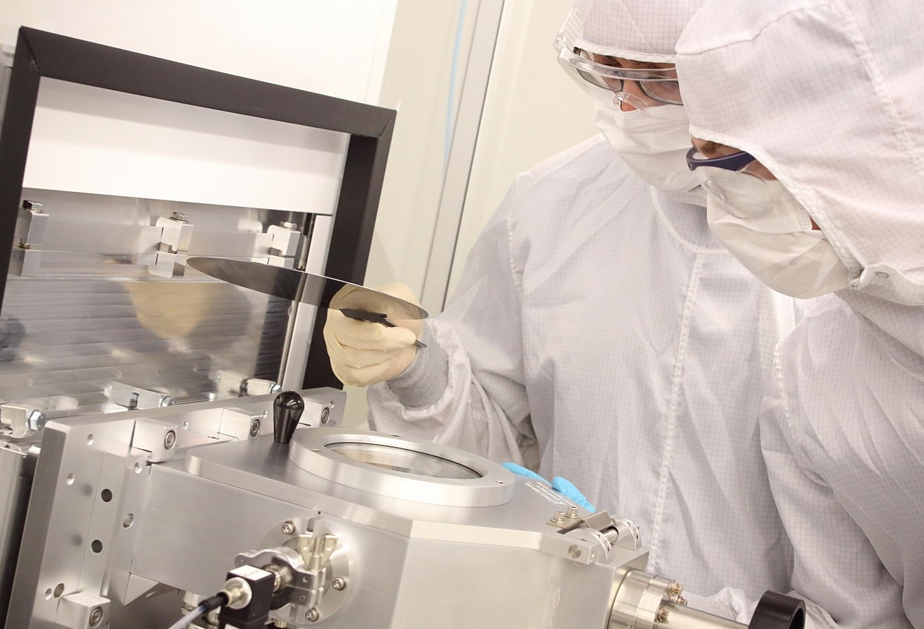
The ALD process, invented in the mid-1970s, is a method of depositing thin films onto a surface using vapour-phase chemical reactions. For 20 years, this process remained relatively unknown and thus remained unchanged. However, it re-emerged in the early 2000s thanks to the interest of the semiconductor industry and the need for thin films with high conformity and precise thickness control. It is a technique that is controlled by sequential reactions. Each surface reaction allows only one atomic layer of deposition at the time.
Developing ALD technology
At the Luxembourg Institute of Science and Technology (LIST), we aim to translate science into new technologies that can impact people’s lives. And we believe that the way to do it is by using nanomaterials because of their high and undiscovered potential. However, their small size also makes them challenging to work with. During the last years, LIST center of excellence in ALD has gained the knowledge that allows us to work better with them. By now, we can place millions of atoms together to build a new nanomaterial. This is what we call “coating from the atoms up”.
Atomic layer deposition is the missing technology, and every day our tools get more precise, and our knowledge gets sharper. The industries of today and tomorrow are going to need new coating technologies, and will seek the help of experts with the right competencies. The value of our Centre of Excellence in ALD is that once we develop these new tools and technologies and have them available within our cleanrooms, they are there for everybody to use. Anyone, anywhere can work with us and deliver on the promise of nanotechnology.
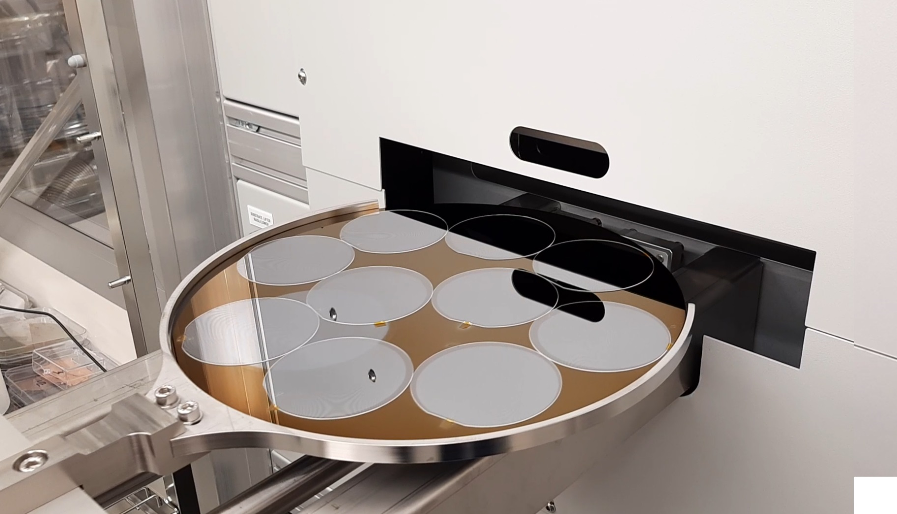
ALD coating technology is valued for its unique conformality and precision even on 3D substrates, but claimed to be slow and not adapted for industrial needs and, therefore, is often ignored. Our Center of Excellence refutes this claim and makes ALD available as an exciting and promising thin film technology for a wide range of industrial applications.
The goals and ambitions of the ALD Center of Excellence
The ALD Center of Excellence is a team. The people working there create a team with a perfect balance between technical skills and scientific knowledge. We work together toward our common vision.
ALD Center of Excellence has the ambition to deposit functional coatings on various types of products. This enables us to make convincing demonstrators for our industrial partners, which are in most cases multinational corporations. At LIST, we possess the equipment which can characterise the developed solutions. This singularity allows us to react faster and adjust our research strategy.
“Ongoing miniaturisation drives our partners to build their coating from the atoms up on flat substrates such as foil or silicon wafer or complex 3D arrangements. Our advanced deposition toolset allows them to create differentiation in their products,” says Noureddine Adjeroud, Engineer at LIST.
The future of atomic layer deposition (ALD)
The demand for atomic thick layer is increasing, as it enables the use of new materials and is compatible with advanced manufacturing. ALD is considered as one of the superior deposition methods, for producing conformal thin films, meaning that the coating will cover all around the object and even in the thinnest holes of porous material. This technology is rapidly evolving, mainly driven by the continuous trend to miniaturise electronic and fabrication of advanced semiconductor devices.
The significance in other applications has become increasingly important and new areas emerge all the time. Many manufacturing companies are looking into ALD and our Center of Excellence is getting more and more requests coming from various manufacturers as they are interested in seeing what ALD could provide for them. The innovation race in the industry is often so competitive that it is hard for them to discuss openly what kind of substrates or coating there are interested in. That is why working under a nondisclosure agreement (NDA) is our standard practice.
Have there been any new developments?
ALD Technology and the LIST ALD Center of Excellence has the potential to push the frontiers of research. As a key member of this Centre, Noureddine uses the benefit of his expertise on the subject to testify throughout the article and focuses on some recent LIST projects that got publication last year:
- Our team presented an innovative approach using gaseous oxygen during the ALD growth of metal-oxide film such as ZnO thin films. Oxygen helps to overcome the challenge of obtaining preferentially (002)-oriented and resistive films at temperatures below 180°C, which is a prerequisite for achieving a piezoelectric response in ZnO thin films and for preventing leakage currents. The paper “Controlling electrical and optical properties of zinc oxide thin films grown by thermal atomic layer deposition with oxygen gas” was published in April 2020, DOI: 10.1016/j.rinma.2020.100088.
- Dealing with several thermodynamic parameters (such as the growth temperature and purging time) a high-quality AlN thin film with the (002)-oriented film and a substantial piezoelectric response was obtained for the first time by PE-ALD at a (low) temperature of 250°C. The process proposed, with the highly conformal growth of aluminium nitride, opens up pathways to design novel piezoelectric functional materials for micro-electro-mechanic system devices with complementary metal-oxide-semi conductor process temperature compatibility. The paper “A film-texture driven piezoelectricity of AlN thin films grown at low temperatures by plasma-enhanced atomic layer deposition” was published in June 2020. DOI:10.1063/5.0011331.
- Elucidating the growth mechanism of ZnO films by Atomic Layer Deposition with Oxygen Gas via isotopic tracking, published in mars 2021, DOI: 10.1039/D0TC05439A
- Our team reported on the evidence of negative capacitance values in a system consisting of metal-semiconductor-metal (MSM) structures, with Schottky junctions made of zinc oxide thin films deposited by ALD on top of platinum interdigitated electrodes (IDE). A complete study was carried out by measuring the capacitance and conductance characteristics under the influence of both dark and light conditions, over an extended range of applied bias voltage and frequency. Thus, we propose a simple device where the capacitance values can be modulated over a wide frequency range via the action of light and strain, while using cleanroom-compatible materials for fabrication. These results open up new perspectives and applications for the miniaturisation of highly sensitive and low power consumption environmental sensors. Evidence of Negative Capacitance and Capacitance Modulation by Light and Mechanical Stimuli in Pt/ZnO/Pt Schottky Junctions, published in March 2021, DOI: 10.3390/s21062253.
The ALD team consists of several scientists (Dr Petru Lunca Popa, Dr Jérôme Polesel-Maris, Dr Didier Arl, Dr Renaud Leturcq, Dr Guillaume Lamblin, Kevin Menguelti and our talented PhD students.
References
- FNR PRIDE MASSENA 15/10935404/MASSENA pour les parties AlN et ZnO.
- Et FNR CORE project PSSENS C16/MS/11349047 pour la partie ZnO et capteurs de contraintes.
Please note: This is a commercial profile
© 2019. This work is licensed under CC-BY-NC-ND.


