
The Danish Technological Institute are working on the frontier of technologies for the printed electronics industry, and explain here their areas of expertise
Printed electronics combines existing print technologies with novel conductive, dielectric and sensing materials. This combination can create electronic components with unique character-istics such as making them lightweight, ultra-thin, flexible and even stretchable.
As a result, printed electronics is facilitating the integration of electronics into a range of new and existing applications, such as construction, smart packaging, smart textiles, eHealth and automotive parts, just to name a few.
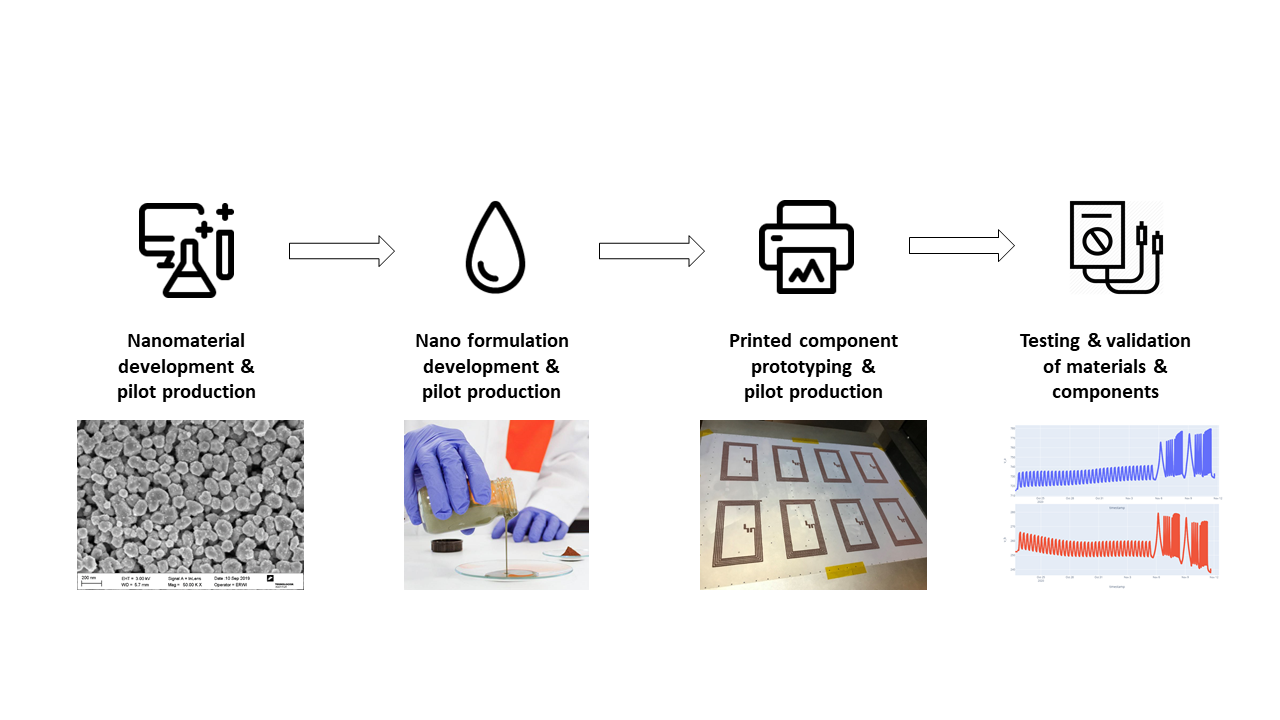
The Danish Technological Institute (DTI) is supporting this by both having state-of-the-art facilities as well as strong European collaborations with the leading technology organisations, through the European projects LEE-BED, BioMAC and SocKET. The areas of expertise at DTI are shown in Figure 1.
Tailored nanomaterials are paving the way to material and costs savings
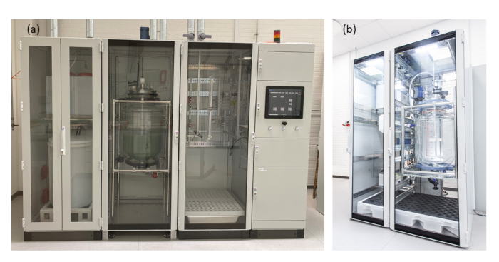
DTI Printed Electronics has been focusing development on reducing development times as well as automating large scale production of nanomaterials usable for printed electronics. Figure 2 shows our nano copper production reactor and filtration facility, which can produce and clean up to 10 kg copper nanoparticles within a single day. The reactors are PLC controlled, fully automated and have in-line pH and temperature monitoring capabilities. Using these reactor technologies, it is now possible to push production costs down to raw material costs, which is needed in order to compete with existing conductive material on the market, i.e. silver flake technology.
Furthermore, DTI is working with alternative materials such as copper nanoparticles and nanowire technologies, both for material and cost savings and for transparent and stretchable ink applications.
Industrial DEMO: Invisible electronics & lighting
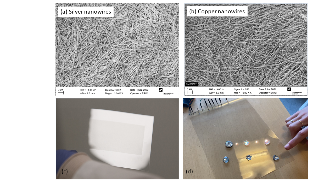
A prime example of the type of innovation DTI can perform is our invisible electronic DEMO. Transparent conductive materials are in high demand in applications such as automotive, wearables and organic solar cells. DTI has developed silver and copper nanowires, a nanowire based conductive ink and a production process for highly transparent electronics. In Figure 3 (a&b) scanning electron microscopy images are shown of nanowires, which have diameter between 50-100nm and lengths from 10-100µm. In Figure 3c, one can see a PET foil coated with a nanowires coating, highlighting the transparency.
Typically, the optical transmission is between 80-90% with sheet resistances below 50 Ω sq. In figure 3d, a prototype fully transparent circuit is shown, where a nanowire coated foil has been micromachined using an excimer laser to form an electric circuit. The developed process results in a virtually invisible circuitry, where, in this case, touch sensing, LED lighting and a thermal couple have been integrated. On top of the foil, Swarovski crystals have been placed to enhance the ascetics of the touch and LED lighting functionalities.
Standardised Testing
A crucial part of the development of electronics is testing. At DTI we have facilities for standardised environmental and mechanical testing with real-time monitoring. Figure 4(a), shows real-time monitoring of the resistive properties of two different types of carbon-based inks while cycling over a period of over two weeks. The data shows how both materials drift with time, due to humidity trapping within the carbon material. In Figure 4(b) real-time measurement of mechanical stretching of a screen-printed silver wire on a stretchable substrate are shown.
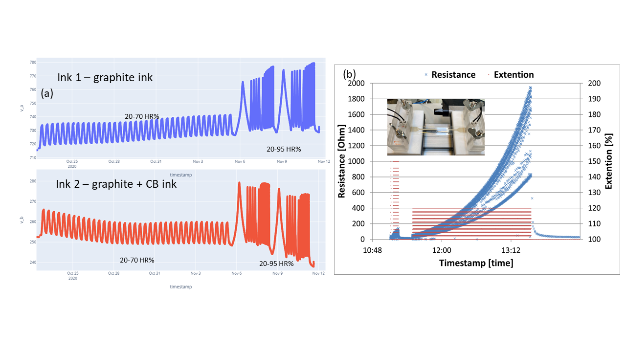
First, the wire is stretched 50% for 10 iterations, then 20% for 200 iterations. The resistance of the wire increases steadily from around 20 Ohms to over 1800 Ohms. However, after stretching is stopped, the resistance falls to below 50 Ohms again within some hours. This highlights the complex behaviour of printed wires when integrated into stretchable applications, such as clothing or medical bandages.
Closing Remarks
Printed Electronics materials and technologies are in growing demand. Danish Technological Institute can assist you with how and when printed electronics is the right technology for your applications and can provide proof of concept, prototyping and even pilot production services. DTI has activities across the entire value chain and has an extensive European network to provide the right partner for your needs.
If you would like to know more about our technologies, please visit our website and contact us today.
Please note: This is a commercial profile
© 2019. This work is licensed under a CC BY 4.0 license.


Screen printing is one of the simplest and most cost effective techniques used by electronics manufacturers. This technique is based on a woven screen that has different thicknesses and thread densities.