
Here, we learn why Horizon 2020 project LEE-BED is currently Europe’s one stop shop for printed and embedded electronics services and infrastructure access
The demand for flexible, stretchable and embedded electronic technologies is growing rapidly due to the growth in IoT, eHealth, automotive, wearables and other similar application areas. At the core is printed electronics, which uses printing technologies such as screen, flexographic and inkjet printing, together with functional inks to fabricate electronics directly onto plastic foils, paper or textiles.
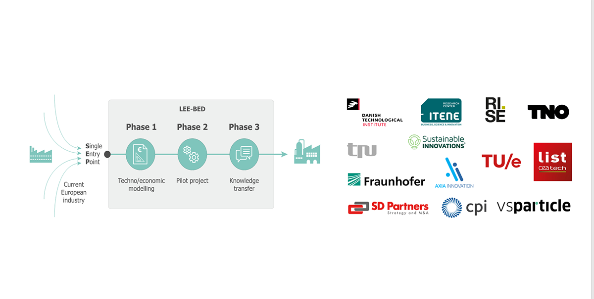
The goal of the Horizon 2020 project LEE-BED (Open Innovation Test Bed for the development of nanomaterials for lightweight and embedded electronics) is to form an open innovation test bed (OITB), which provides services and pilot line access through a simple and straight forward single entry point (SEP).
This article will describe how the SEP works in practice, what services and pilot lines are accessible and finally, the industrial end-user cases that LEE-BED are working with.
What are printed and embedded electronics?
The main idea is to use conventional printing technologies, such as screen printing, flexographic printing and, in the future, inkjet printing, to print electronic layers onto flexible substrates. This allows for high volume manufacturing, using large area sheet-2-sheet or roll-2-roll printing systems, which reduce manufacturing costs, increases sustainability as well as decreases the size and weight of the electronics. Furthermore, printing onto foils facilitates embedding electronics functionalities into new products, where rigid printed circuit board (PCB) technologies cannot.
One of the main bottlenecks for the technology is the availability of printable functional materials. Currently, many commercial conductive and insulating inks exist, which are used for making standard electronics, however, new types of inks are needed to print more complicated components, such as sensors, increase stretchability for wearables, etc. This requires working across the entire value chain, with several different types of industries, materials suppliers and research organisations.
How does LEE-BED work?
The overall concept of LEE-BED is shown in figure 1. Through the Single Entry Point (SEP), European stakeholders can gain access to services and pilot lines, dedicated to printed electronic activities. The SEP is a website where you can access information about LEE-BED services and pilot lines, partners, industrial end-user cases and other useful information. LEE-BED consists of 13 European organizations/ specialized companies, offering over ten tailored services and 12 infrastructure pilot lines.
On the website, there is a simple sign-up page, which is the starting point for LEE-BED access. Once you have signed up, a Project Manager will contact you personally and lead you through the process, consisting of three phases. Phase one consists of a technical and economic assessment, a life-cycle and safety assessments and a patent mapping service. The goal of phase one is to provide the client with a technical solution, as well as useful information about:
- How much would it cost to develop and eventually implement/upscale production?
- What is the sustainability and safety of the materials and processes involved?
- What is the IPR landscape?
In this way, the client can make an informed decision before entering phase two and performing a pilot project. For SMEs wanting to access LEE-BED services and pilot lines, there is a final service, which assists the client to procure economic funding, either through national or European funding schemes.
In phase two, the client will gain access to the LEE-BED pilot lines. The Project Manager will coordinate the pilot project and be the main point of contact. Through the pilot project, clients will be able to perform both development and pilot production activities, across the entire value chain using three categories of pilot lines, namely nanomaterial, nano-enabled formulation and component pilot lines. LEE-BED has 12 pilot lines, through collaboration with eight European partners across seven different countries. More information about each pilot line can be found here.
Finally, after the client has finished a pilot project, they will enter phase three, consisting of four knowledge transfer services. These services include IPR management and patenting support, standardisation, final Business Plan development and assistance getting in contact with venture capital.
Industrial end-user cases
To validate the LEE-BED services and pilot lines, four end-user cases have been defined together with four European companies. The latest results of each industrial end-user case can be found here.
MAIER Group works with the development and production of plastic panelling for the automotive industry and LEE-BED is developing automotive interior components, with fully embedded electronic functionalities, such as touch sensing and LED lighting, which provide a high added aesthetical value to these components.
ACCIONA is a construction company working with composite-based materials. LEE-BED is collaborating with ACCIONA to find solutions for embedding wireless sensors systems into their composite building elements for both asset tracking and process monitoring. This will directly contribute to reduce maintenance costs and increase safety.
Swarovski KG is a manufacturer of attainable luxury products including crystal, jewellery and other decorative products (e.g. for the automotive sector). LEE-BED is assisting Swarovski with adding printed electronic functionalities, such as touch sensing and lighting, into their well-known crystal technology. LEE-BED has developed novel nanomaterials, ink formulations and production processes.
Grafietic are producers of packaging and labelling. LEE-BED is developing novel materials and printing processes to develop smart labels, which are applied to packaging solutions. The purpose is to explore possibilities, such as printed displays to indicate the best before date, printed RFID antenna, to inform about temperature and possibly electroluminescent displays.
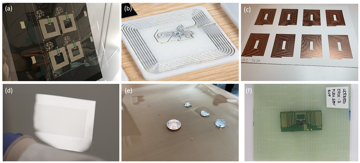
Figure 2 shows some of the highlights of results produced through LEE-BED pilot projects.
LEE-BED open access
LEE-BED is now opening its services and pilot lines to the public. If you think LEE-BED could assist your work, we invite you to apply and be part of the LEE-BED competition to receive a full phase one evaluation, free of charge. Find more information on our website.
This publication is supported by the European Union’s Horizon 2020 research and development programme under grant agreement No. 814485.
Please note: This is a commercial profile
© 2019. This work is licensed under CC-BY-NC-ND.


