
Francesco Crivelli, PhD from CSEM Center Alpnach in Switzerland, discusses the automated 3D inspection of micro-electro-mechanical systems in this robotics & machine learning focus
Today, micro-electro-mechanical systems (MEMS) are ubiquitous as actuators and sensors in applications ranging from smartphones to automotive parts and medical devices, including implants. In these highly competitive markets, it is crucial to production yield and quality. It is, therefore, desirable to detect defects early in MEMS production with high accuracy and low strain on human workers as it saves resources on labour and raw materials. With increasing needs for miniaturisation and improved manufacturing know how, MEMS are becoming smaller and more three-dimensionally complex. Optical inspection with conventional methods such as microscopes can be limited in throughput as the MEMS extend over the depth-of-focus of these instruments. Also, MEMS inner layers are invisible.
The solution developed in the European project CITCOM consists of two automated inspection instruments, for the quality control of complex, highly miniaturized 3D MEMS. High depth-of-focus images are acquired by plenoptic camera and X-ray. These images undergo automated defect recognition, requiring minimal human intervention. These systems are contactless non-destructive testing units that scan entire MEMS wafers or single components and can be applied at any stage of the production and assembly process. Finally, the operator is presented with the inspection results.
A fully integrated, industry-ready pilot line
Today, two inspection systems are ready to be used and evaluated within a MEMS manufacturing facility. A 3D vision in-line system developed to inspect 100% of production is flanked by a side-line X-ray system.
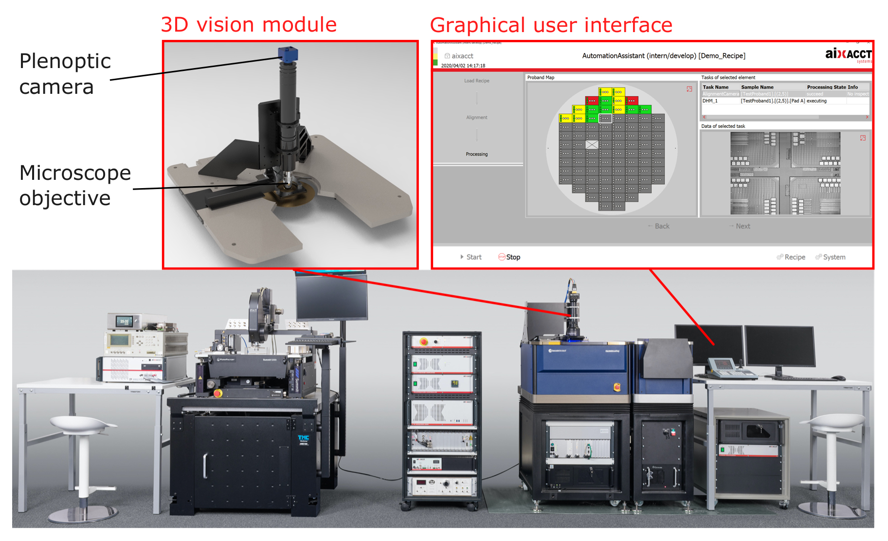
The first consists of a conventional micro-electrical wafer prober, which has been retrofitted by aixACCT Systems GmbH with a plenoptic camera (Figure 1). These cameras developed by Raytrix GmbH capture the information of light ray’s origin in 3D space, via a microlenses array placed closely in front of a conventional photosensitive chip. After calibration of the camera, the imaged object is computationally reconstructed, resulting in a 3D depth map and a fully focused image (Figure 3). This technology resolves details at the micron scale in 3D, with high throughput, up to 80 fps. The chosen cameras are compact and have an extended depth of focus compared to microscope cameras with similar optical properties because the microlenses have various focal lengths. The combination of all these advantages renders this technology ideal for MEMS inspection.
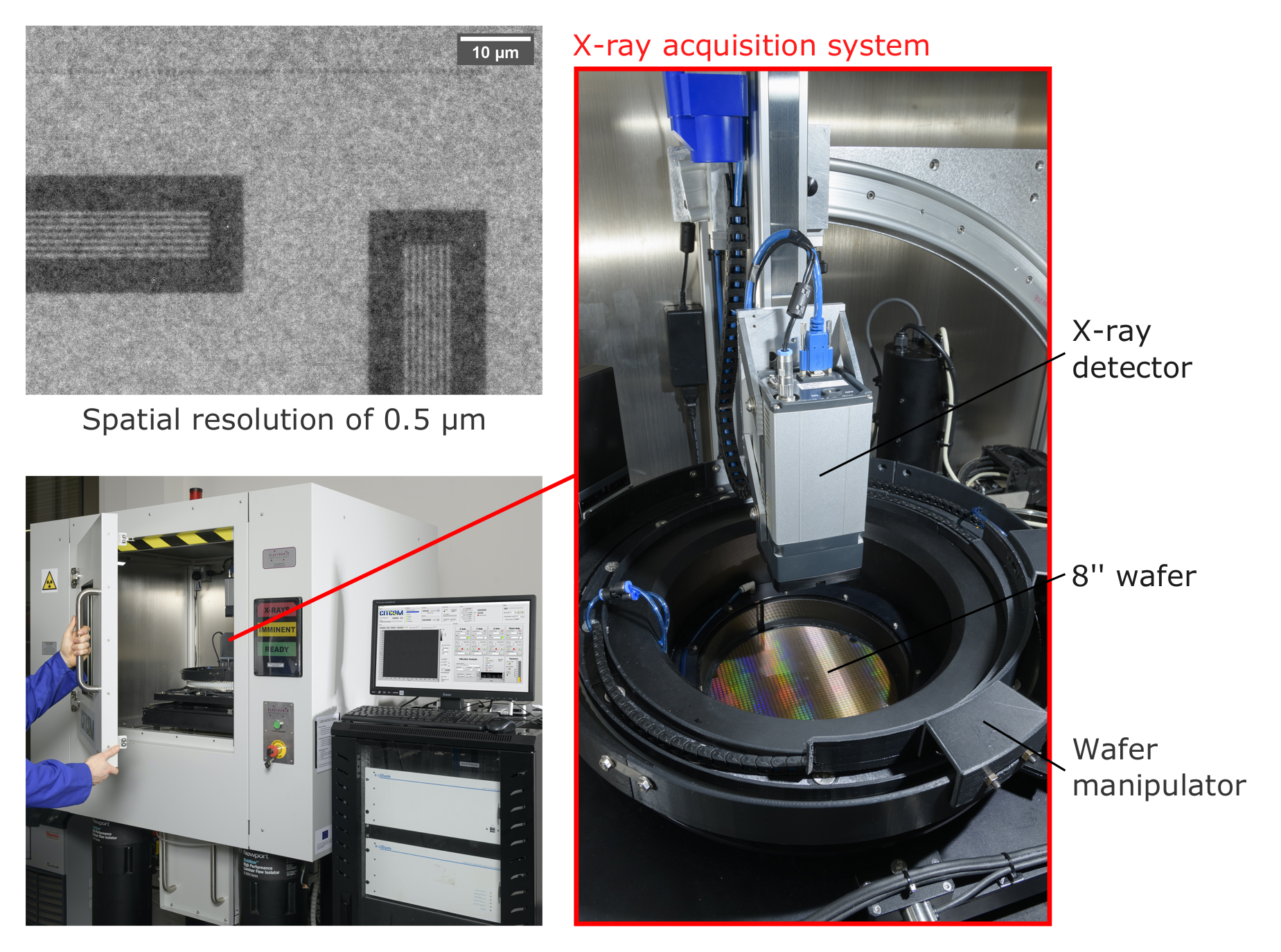
The X-ray system mainly consists of the X-ray source, detector and manipulator, integrated by TWI Ltd (Figure 2). Optimisation of the system resulted in a maximal spatial resolution of 0.5 µm, enabling detection of sub-micron defects. A nano focus X-ray tube source Excillum NanoTube N1 was further enhanced by Excillum AB. X-rays are detected by a large 5.5MP Charge Integrating Detector. The manipulator was designed by InnoTecUK Ltd. and can manoeuvre up to 8” wafers with three-axis translations and one axis full rotation.
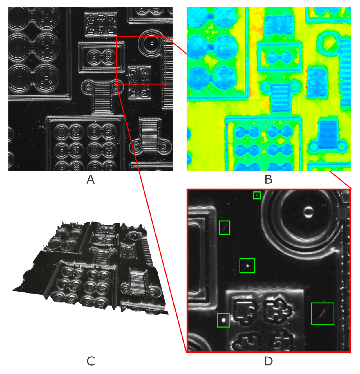
Dedicated software automates wafer handling and inspection on both systems. A common backend software guarantees integrated control of the imaging hardware, steers the image analysis workflow and relays information to all components. The automated analysis includes image reconstruction, stitching and noise filtering as well as metrology and automated defect recognition (ADR). ADR, developed by the Brunel Innovation Centre, applies Deep Learning (faster R-CNN Inception v2 COCO) to detect anomalies such as defects and foreign particles (Figure 3).
Both systems will be running at the industrial partner Microchip Technology Caldicot Ltd. for evaluation.
Significant economic and environmental benefits
By applying 100% in-line inspection and providing the tools to identify defects at the early production stage, the proposed approach has the potential to significantly improve production quality and efficiency.
The economic benefit of the system was shown by benchmarking with state-of-art methods at Microchip Technology (i.e. human experts with high magnification microscopy). Life Cycle Assessment and Life Cycle Costing also showed a positive environmental impact. The results suggest that the increased efficiency, combined with reduced electricity and waste guaranteed by the CITCOM system, could reduce operation and maintenance costs by up to 76%. Moreover, a significant potential decrease of 40% in environmental impact could be expected in most categories (e.g. climate change, energy use, eutrophication). Finally, different recycling scenarios to be associated with the CITCOM technology have been proposed, to promote a circular economy approach.
CITCOM involves 12 European industrial partners and RTOs coordinated by CSEM SA. The project has received funding from the European Union’s Horizon 2020 research and innovation programme under grant agreement No. 768883. CSEM is a Swiss RTO that operates worldwide. With more than 500 employees, the organisation develops high-tech for industry in various markets. Focus areas are “Precision Manufacturing”, “Digitalization”, “Clean Energy”. More information is available under.
*Please note: This is a commercial profile


