
Here, Dr Dimiter Prodanov from IMEC explains the final outcomes and perspectives of the NanoStreeM project, including comments on nanomaterials and risk
Nanomaterials are used in many industrial applications. Desirable characteristics, subject to optimisation, can include increased strength of the nano-enabled material, its chemical reactivity, or altered electrical properties. Engineered nanomaterials, ENMs, are incorporated in a wide variety of consumer products: from cosmetics and paints to sportswear, mobile phones, computer chips, and batteries. Such materials represent bottom-up nanotechnology, where particles, fibres or surfaces are synthesised from molecules. In contrast, top-down nanotechnology can be exemplified by semiconductor processing, where nano-scale features are patterned with exceptional precision on macroscopic objects.
In the concrete case of the semiconductor industry, there are more than 200 chemical compounds consisting of elements, such as silicon, germanium, copper, gold, hafnium, indium among many others, which are present in most computer and mobile phone chips. In some chip manufacturing processes, ENMs enable superior yields and performance. Other examples include the solar cell industry and energy storage, where a number of diverse materials based on rare earth elements are used. Every one of these applications requires unique expert insight into the possible consumer, occupational or environmental hazards.
Nanomaterials and risk
It is generally anticipated that the recently developed first generation and the upcoming second-generation of active nanomaterials pose challenges for assessing their risk. Therefore, a variety of new risk assessment tools have been developed. Acceptance and use of one or another risk assessment framework can have a wide range of economic and safety repercussions, therefore it is of considerable science policy interest. For example, in the European Union, nanosafety research has been supported throughout the last three EU Framework Programmes. Whereas only five nanosafety projects were funded in the 6th Framework Programme, around 50 projects and initiatives on nanosafety were funded in the 7th Framework Programme, between 2007 and 2013.
By 2018, 19 projects had been funded under H2020. In the U.S., the National Institute of Occupational Safety and Health (NIOSH) is the leading federal agency conducting research and providing guidance on the occupational safety and health implications plus applications of nanotechnology. International regulatory science efforts are coordinated by the Organisation for Economic Co-operation and Development (OECD). However, it should be noted that partially because of this vigorous science policy interest, the number of publications dealing with the toxicology of nanomaterials has increased tremendously, although most studies are not directly applicable in the industry setting for the risk assessment of Engineered Nanomaterials (ENMs).
Reflections on the NanoStreeM project
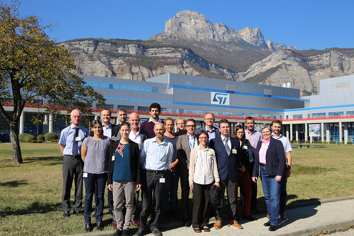
The NanoStreeM project, funded under H2020, gathered 14 partners from 6 European countries. Throughout its operation from 2016 till the end of 2018, the NanoStreeM project consortium defined a road map of occupational safety of nanomaterials in nanoelectronics where we have identified the existing gaps in the present knowledge and formulated a number of recommendations for their mitigation. Definite needs for competencies development were established in terms of informing about the physicochemical properties of nanomaterials, a dedicated nanotoxicology knowledge base, and about the limitations of the traditional occupational chemical risk assessment. To meet these needs, the project composed nanosafety training packages, as one of its major outcomes. As a final outcome, the project partners Tyndall, The French Alternative Energies and Atomic Energy Commission (CEA), and Imec composed three dedicated training courses focusing on semiconductor industry processes and the cleanroom environment. Developed training packages have been used by the semiconductor industry and the partnering institutions after the project ended and are available on request from the European Semiconductor Industry Association.
On one hand, the assessment of risk in the field of nanotechnology requires an integrated multidisciplinary approach due to the complex and cross-disciplinary framework for materials and activities at the nanoscale. On the other hand, the safety of nanomaterials and nanotechnology cannot be considered on a case-by-case basis, as this will effectively block innovation. A systematic framework for risk governance should be centred on generic principles, such as Safe by Design. Conversely, concrete implementations of such principles can be sector-specific.
In the engineering context, Safe by Design can be implemented as the integration of hazard identification and risk assessment methods early in the design process to eliminate or minimise the risks of harm throughout the construction and life of the product being designed. Safe by Design includes three components: safe design, safe production, and safe use. In the context of the semiconductor industry, “safe design” translates to the development of processes, where the used nanoparticles have known hazards. “Safe production” entails a reduction of process hazards at identified hotspots of risk. “Safe use” ought to consider issues, related to recycling and end-of-life. Such knowledge, then may be used to inform design choices, for example in the integrated circuit design.
The NanoStreeM project demonstrated that the nanoparticle emissions in the normal operation mode of cleanroom processing tools are not likely to occur. Therefore, future studies in the semiconductor industry should focus on the assessment of the full lifecycle, including the environmental impact, product end-of-life, and recovery of valuable elements through recycling. Finally, the NanoStreeM project has identified some key challenges and data gaps, which the industry is facing. In the first place, it is the lack of reliable data on nanoform toxicity. The persistence of such gaps inadvertently leads to uncertainty in regulations. The publication of the REACH Annex amendments in 2019, in which requirements for nanoforms are described, is a major step towards increased regulatory guidance. Nevertheless, the implementation will take many years to fully generate data for increased industrial confidence.
Secondly, risk assessment methods for nanomaterials are far from mature, which makes their application very difficult in an industrial setting. Therefore, innovation guided by the Safe-By-Design principle must be aided by ongoing and future regulatory research. The H2020 programme funds three ongoing projects focused on developing the European Risk Governance Council that would provide independent advisory services of importance to industry in general and specifically to the semiconductor industry. The latest development in the field is linking risk governance with designing safe products. Most recently, H2020 funded four consortia to work specifically on nanosafety issues.
Additionally, it will be important to identify appropriate sources of information and communication channels for all actors along the supply chain, including the general public. Finally, the findings of the project and its actionable recommendations have been recently published in Frontiers of Public Health.
Acknowledgement
The NanoStreeM (Nanomaterials: Strategies for Safety Assessments in Advanced Integrated Circuits Manufacturing) project receives funding from the European Union’s Horizon 2020 Research and Innovation Programme under grant agreement n° 688794.
*Please note: This is a commercial profile


