Nanoscience Related Content
Deep Learning Approaches to Electron Microscopy
Electron microscopy is the primary method for analyzing nanostructures. Senior researcher Thomas Willum Hansen discusses the new challenges in this field.
The challenges of nanophotonics in modern optical technologies
Toralf Scharf, Senior Scientist/Faculty Member at École polytechnique fédérale de Lausanne EPFL identifies the exciting challenges of nanophotonics where modern optical technologies are concerned.
The governance of emerging nano-risk in the semiconductor industry
Dr Dimiter Prodanov from IMEC sheds light on the governance of emerging nano-risk in the semiconductor industry in this summary workshop report.
Nanomedicines: Depicting human health risks hindering clinical translation
Cecilia Van Cauwenberghe from Frost & Sullivan shares her expertise on the world of nanomedicines, with a special focus on depicting human health risks hindering clinical translation.
DTU – Small is beautiful
This compelling document focuses on attention to detail, hence its apt title, ‘small is beautiful’. This intriguing e-book is all about nanoscale imaging research and within that, the fascinating field of electron microscopy
Innovators race to find sustainable polymer-based materials
Jennifer Unsworth, Senior associate and patent attorney at Withers & Rogers LLP shares her expertise on the race for innovators to find sustainable polymer-based materials
Nano safety, advanced materials for the semiconductor industry and governance of nano-related risk
Dr Dimiter Prodanov from IMEC vzw shares his views on the fascinating world of nanomaterials including the governance of nano-related risk
Atom-by-atom: Gas to solid reactions visualised in real time
Professor Jakob Birkedal Wagner, Scientific Director at the Center for Electron Nanoscopy at DTU Cen, provides an absorbing insight into gas to solid reactions that are visualised in real time, atom-by-atom
Nanowires, doping and electron holography
Elisabetta Fiordaliso of DTU CEN discusses Nanowire technology and how it works, something which is decreasing the dimensions of our electronic devices more and more.
The density of integrated electronic components in the semiconductor industry continues to increase, resulting in shrinking dimensions of individual devices. Many different semiconductor materials are...
Integrating nanomaterials safety data so that it is Findable, Accessible, Interoperable and Re-usable
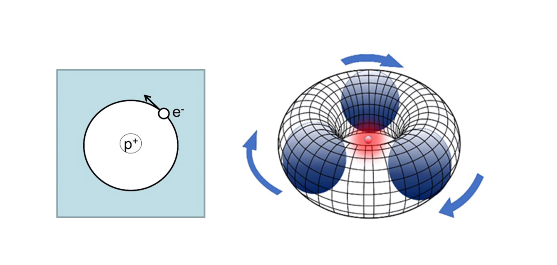
Professor Iseult Lynch from University of Birmingham, School of Geography, Earth and Environmental Sciences explores the amazing opportunities offered by nanotechnologies
Nanotechnologies and the ability to manipulate matter at the nanoscale (1-100nm) have opened up amazing new opportunities for industry and consumers. Nanotechnology has been identified as a key enabling...
Natural colours from cellulose
Silvia Vignolini, Reader in Chemistry and Biomaterials at University of Cambridge explores the wonderful world of colour and how it affects our perception and mood
Colour is a powerful communication tool, it deeply affects our perception of the world, stimulating our senses. It is not by chance that since the...
Nanomaterials in the semiconductor industry: An end-user industrial perspective
Dr. Dimiter Prodanov from Imec gives an end-user industrial perspective on the vital role of nanomaterials in today’s semiconductor industry and their safe use
Nanomaterials are broadly defined as those materials that have a certain percentage of particles at the nanoscale, between 1 and 100 nanometres1. While the size cut-off...
Transmission electron microscopy to see ‘functionalities’ and ‘material property interactions’
Senior researcher at Center for Electron Nanoscopy at DTU CEN, Takeshi Kasama reveals the institution’s expertise around transmission electron microscopy
Nanomaterials for energy storage: Powering our world
Nanomaterials offer significant advantages for energy storage applications, as Professor Valeria Nicolosi’s research is demonstrating.
Imaging magnetic nanoparticle superstructures
The Center for Electron Nanoscopy at DTU discusses research into the magnetization of nanoparticle superstructures, advancing their use in modern technology
Magnetic materials at various length scales are everywhere in modern technology. From cars, trains, airplanes and wind turbines (1 mm – 1 m), to cellphones, computers, memory drives and...
Applied nanosciences for printing technologies
Applied nanosciences offer new possibilities for printing and processing, as outlined by Prof. Dr. Silvia Schintke from Heig-VD/HES-SO Switzerland
Nanoscale imaging research: Why is it useful?
The Center for Electron Nanoscopy’s Professor Jakob Birkedal Wagner highlights the strides being made in nanoscale imaging research
What is the importance of mechanical systems?
The University of Applied Sciences’ research group discuss the challenges of mechanical systems and the benefits they bring to everyday life
Lighting up future materials and devices
Stefan Hecht at Humboldt-Universität zu Berlin outlines how light-based technologies will spark innovation in material science and nanotechnology
The emergence of life and our existence is inevitably bound to the sun as the prime energy source for our planet. Photosynthesis provides the basis for the continuous production of biomass, which...